

KLA: A Perfect Business at an Imperfect Price
KLA may be the ultimate semiconductor tollbooth, just not at 49x earnings

TL;DR:
KLA’s economics improve as semiconductor complexity rises, rare for industrials
Services + data moat + packaging create a structurally stronger model
Expected returns look flat unless the bull case is more likely than the market assumes
In the spring of 1997, a team of engineers at KLA-Tencor gathered in a conference room in Milpitas, California, to confront an uncomfortable reality. The semiconductor industry was migrating from the 350-nanometer to the 250-nanometer process node, and defect rates were spiraling out of control. Chipmakers who had previously treated optical inspection as a nice-to-have, a quality check bolted onto the end of the manufacturing line, were suddenly discovering that invisible particles, measured in fractions of a human hair’s width, could destroy entire wafer lots worth millions of dollars.
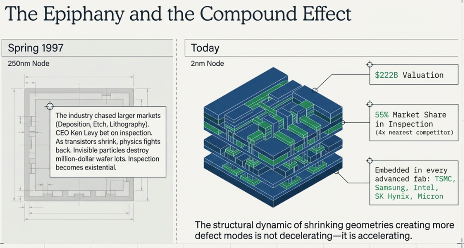
What happened next defined KLA’s strategic identity for three decades. Rather than diversifying into the larger, more glamorous equipment markets, deposition, etch, lithography, CEO Ken Levy doubled down on inspection. The bet was simple but counterintuitive: as transistors shrank, the laws of physics would increasingly fight back. The probability of killer defects would rise exponentially, making inspection not just important but existential for every chipmaker on earth. Every competitor chasing bigger markets would eventually have to come to KLA for the quality assurance layer.
By 2000, KLA owned more than half the wafer inspection market. It has never relinquished that position.
Twenty-nine years later, the bet has compounded beyond anything Levy could have imagined. KLA Corporation is a $222 billion company trading near all-time highs. Its process control tools are embedded in every advanced fab on earth, TSMC, Samsung, Intel, SK Hynix, Micron. Its 55% market share in inspection is more than four times its nearest competitor. And the same structural dynamic that made KLA essential in 1997, shrinking geometries creating more defect modes, is not decelerating. It is accelerating.
The 2-nanometer node, high-bandwidth memory stacks, and advanced chiplet packaging are the 1997 moment compounded across three dimensions simultaneously. The question this essay tries to answer is whether KLA is just a beneficiary of a strong capital expenditure cycle, or whether it is the rare industrial company whose economics structurally improve as its industry gets harder. And if the answer is yes, whether the stock price already knows it.
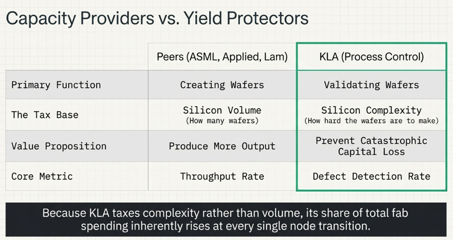
What KLA Actually Sells
To understand why KLA’s position is unusual, you have to define what the company actually does, and it is not what most people think.
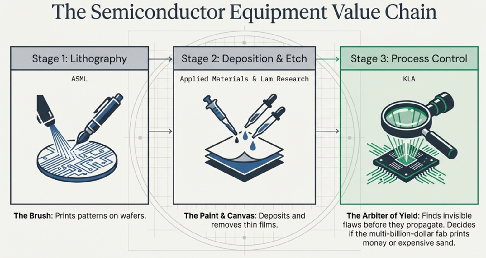
A semiconductor foundry like TSMC does not buy a KLA machine to make chips. It buys ASML machines to print patterns on wafers. It buys Applied Materials and Lam Research machines to deposit and etch thin films. These are the tools that build the chip. The specific job a customer hires KLA to do is different: find the invisible flaw immediately, before it propagates through dozens of subsequent process steps, ensuring that the multi-billion-dollar fab actually prints money instead of expensive sand.
The value chain is clarifying. ASML makes the brush. Applied and Lam make the paint and the canvas. KLA is the magnifying glass that decides whether the painting is worth selling.
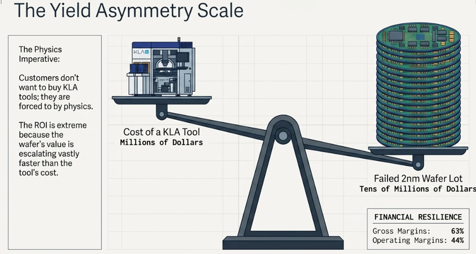
This matters because of the asymmetry embedded in the economics. A KLA tool costs millions of dollars. A failed 2-nanometer wafer lot with advanced packaging can destroy tens of millions. The return on investment for inspection is extreme and rising, not because KLA’s tools are getting more expensive relative to alternatives, but because the value of the wafer being inspected is getting more expensive relative to everything else. This is why customers do not want to buy KLA tools. They are forced to by physics. And it is why KLA maintains 63% gross margins and 44% operating margins regardless of the macroeconomic backdrop. The value is not in the atoms of the tool. It is in the asymmetry of the customer outcome: a small reduction in yield loss can be worth vastly more than the cost of the inspection system that prevented it.
Most semiconductor equipment companies sell capacity, the ability to produce more wafers. KLA sells the ability to make that capacity economically useful. This distinction is critical because it explains why KLA’s share of total fab spending rises at every node transition, a dynamic that has no parallel elsewhere in the equipment stack.
What Changed in the World
The 1997 dynamic never went away. But three things happened simultaneously in the last several years that made it far more powerful.
Logic got harder, in three dimensions
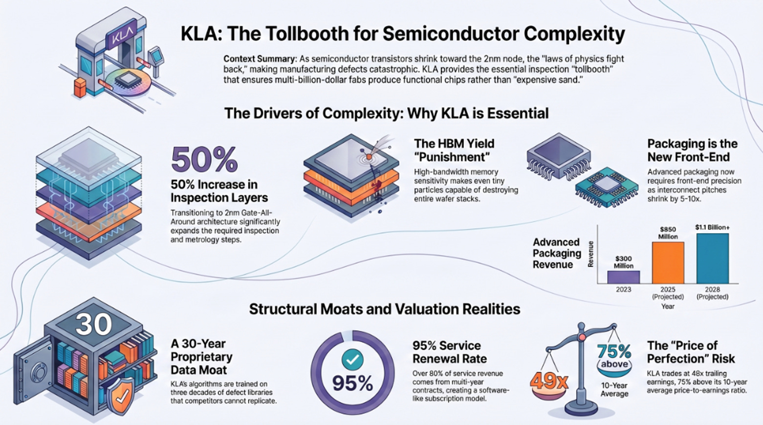
For decades, chipmakers improved performance by shrinking transistors on a flat plane. That era is over. The 2-nanometer gate-all-around transition is the most significant architectural shift in semiconductor manufacturing since Intel introduced FinFET transistors in 2011. Gate-all-around transistors replace the three-sided fin structure with a fully wrapped nanosheet, introducing four to five entirely new process modules and extending total manufacturing steps by roughly 20%. Each new step requires inspection and metrology that did not exist at prior nodes. The result: gate-all-around adds approximately 50% more inspection layers and 30% more metrology layers compared to FinFET.
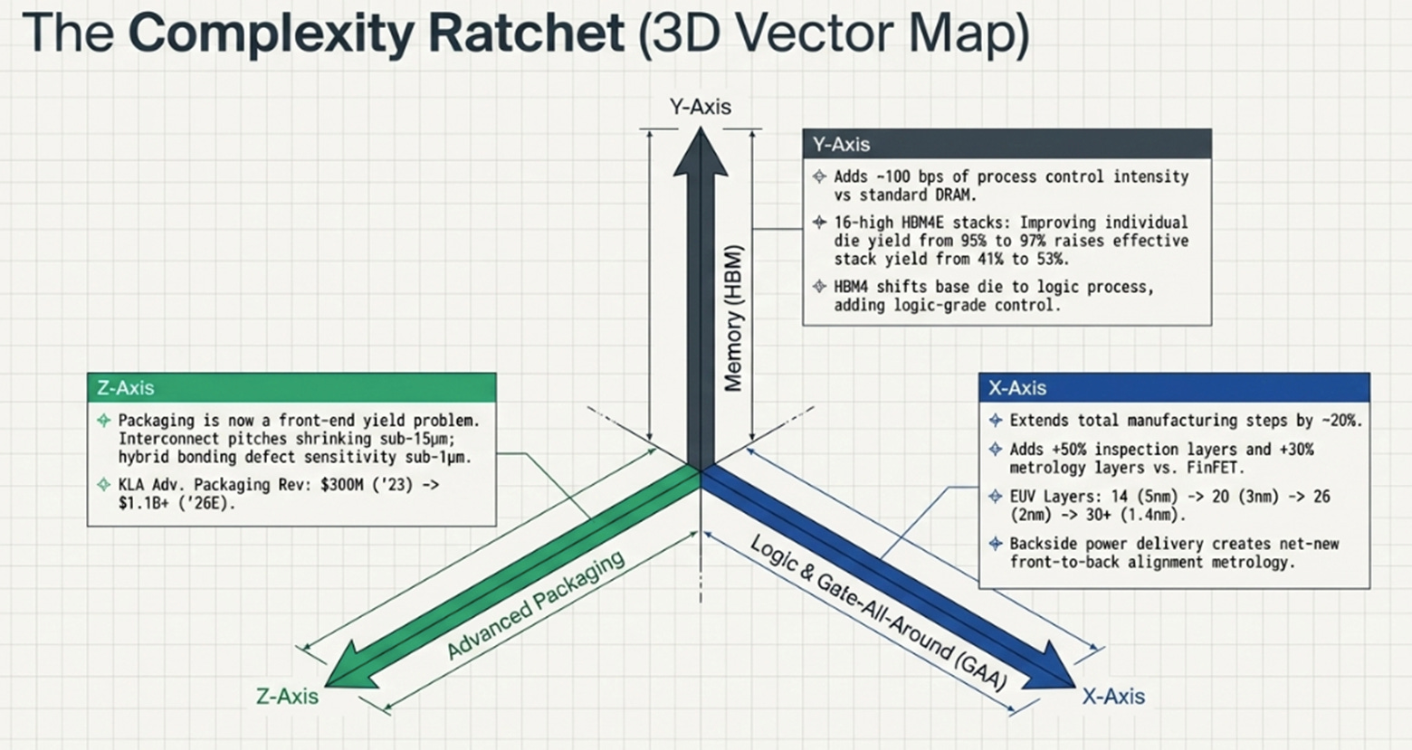
Simultaneously, the number of extreme ultraviolet lithography layers per chip is escalating rapidly, approximately 14 layers at the 5-nanometer node, 20 at 3-nanometer, 25 to 26 at 2-nanometer, and 30 or more expected at 1.4-nanometer. Each additional EUV layer linearly increases demand for reticle inspection and patterned wafer inspection, both areas where KLA holds dominant share.
And backside power delivery, now in production at Intel’s 18A node and ramping at TSMC’s A16, creates an entirely new metrology category that did not previously exist: measuring through the full wafer thickness for front-to-back alignment, where pattern-dependent deformation creates non-linear overlay errors. This is net-new demand that appears in no historical model.
The cumulative effect: each advanced node transition adds 100 to 200 basis points of process control spending as a share of total wafer fab equipment investment. This is permanent and cumulative. Chipmakers cannot reduce inspection steps without accepting lower yields, and lower yields at 2-nanometer geometries are economically catastrophic.
Memory stopped being commodity memory
High-bandwidth memory is not simply more DRAM. It is a fundamentally different manufacturing challenge that transforms back-end memory assembly into a front-end yield problem.
The arithmetic is punishing. A 16-high HBM4E stack, where each individual die has a 95% yield and each bonding step has a 99% yield, produces an effective stack yield of approximately 41%. Improving individual die yield from 95% to 97% raises effective stack yield from 41% to 53%, a 12-percentage-point improvement worth hundreds of millions of dollars in output for a single memory fab. That yield sensitivity directly justifies massive investment in inspection at every stacking layer.
HBM adds roughly 100 basis points of process control intensity compared to standard DRAM. Each HBM wafer undergoes all standard front-end inspection plus multiple additional steps: through-silicon via formation inspection, post-thinning backside inspection, pre-bonding surface inspection, bonding alignment metrology, post-bonding defect inspection, and known-good-die verification. A single one-micron particle trapped between layers during hybrid bonding can cause delamination or void formation, destroying the entire stack.
The roadmap extends through HBM5 and HBM5E into the 2030s. And HBM4 introduces a revolutionary architectural change: the base die shifts from DRAM process to logic process technology, adding logic-grade process control requirements to what was previously a pure memory flow. This is not a one-time capacity buildout. It is a structural shift in how memory is manufactured.
Packaging became a front-end yield problem
For decades, semiconductor packaging was a commoditized, low-margin assembly process, the industrial equivalent of putting a chip in a box. Today, advanced packaging architectures like TSMC’s CoWoS and SoIC shrink interconnect pitches from 90 micrometers down to sub-15 micrometers. Hybrid bonding pushes defect sensitivity from greater than 5 micrometers to sub-1 micrometer, a five-to-ten-times increase that brings front-end-grade process control requirements to what was previously back-end assembly.
KLA’s advanced packaging revenue tells the story: approximately $300 million in 2023, $500 million in 2024, $950 million in 2025, and projected to exceed $1.1 billion in 2026. Market share in advanced packaging has quadrupled in four years. This is not KLA entering a new market with a new product. It is KLA adapting its existing front-end inspection capabilities to back-end packaging processes that now require front-end-like precision.
NVIDIA’s next-generation Rubin architecture will require approximately 2.7 times more interposer area per package than the current Hopper generation, with proportionally more inspection surface. Panel-level packaging, targeting mass production by 2028, will move from 300-millimeter round wafers to large rectangular panels, requiring entirely new inspection tools and creating a replacement cycle on top of growth that no one is currently modeling.
The connecting thread across all three shifts is this: artificial intelligence matters to KLA not through more wafers, but through more complexity per wafer. Larger die sizes, denser packaging, and vertical stacking all increase the probability that a single defect destroys an enormously expensive device. KLA’s tax base is not silicon volume. It is silicon complexity. And complexity, unlike volume, is a one-way ratchet.
The Hidden Quality Shift
The consensus view of KLA is straightforward: it is a best-in-class semiconductor equipment company benefiting from the AI cycle, trading at a deserved premium for its dominant market position. This is accurate. It is also incomplete.
The deeper story is that KLA’s business quality is improving beneath the surface in ways the market has not fully incorporated into its valuation framework. Three shifts are underway simultaneously.
Services are not a footnote
KLA’s services business generated $2.9 billion in calendar year 2025. It has grown for 52 consecutive quarters, more than 13 years without interruption. Over 80% of this revenue comes from multi-year contracts with renewal rates exceeding 95%. Management targets doubling services to approximately $6 billion by 2030, implying a 13 to 15% compound annual growth rate.
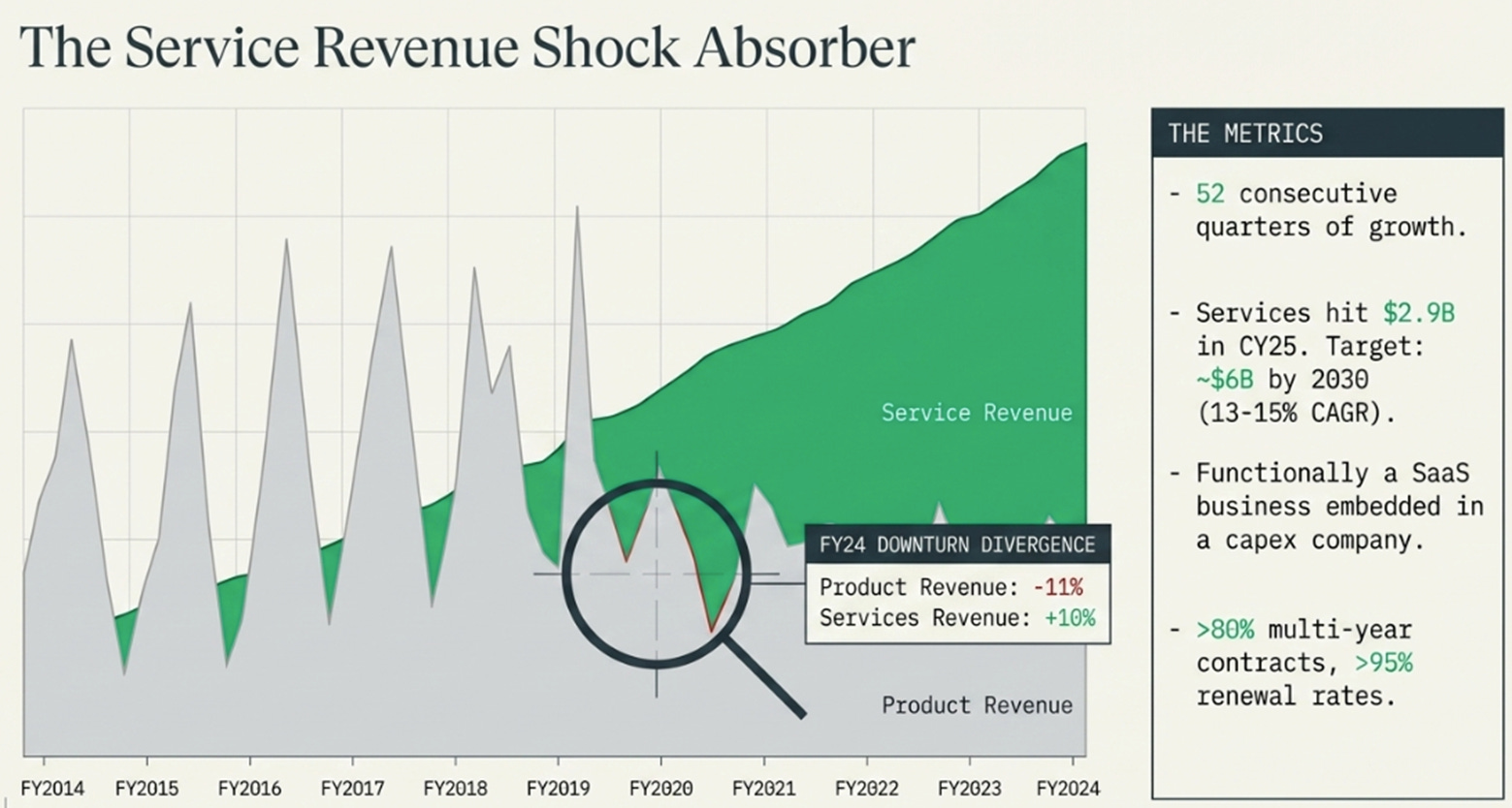
This is, functionally, a subscription business embedded inside a capital equipment company. The market values it at KLA’s blended equipment multiple. If it were a standalone company with these growth rates, this retention, and this margin profile, it would trade at a software-like revenue multiple.
The strategic significance became visible during fiscal year 2024, when KLA’s product revenue declined 11% in a mild WFE downturn. Services still grew 10%. This asymmetry, services grow in downturns because the installed base does not shrink, makes KLA’s overall business fundamentally more durable than the “semiconductor equipment” label suggests. By 2030, services will approach 25% of total revenue at higher margins than systems. The troughs of future downturns will be shallower and more profitable than any prior cycle.
Advanced packaging is not an adjacency
The shift from monolithic chip designs to chiplet architectures means packaging process control demand grows faster than packaging volume, because each successive generation of packaging technology adds inspection steps independent of how many packages are produced. NVIDIA’s migration from CoWoS-S to CoWoS-L, Broadcom’s adoption of CoWoS-L for advanced TPU models, and the emergence of outsourced assembly providers like ASE and Amkor standing up CoWoS lines for the first time, each of these creates greenfield KLA demand that is largely absent from consensus models.
By 2030, advanced packaging could plausibly represent 15 to 20% of KLA’s total revenue, up from approximately 7 to 8% today. That is not a product extension. It is a second core business.
The learning system that strengthens at scale
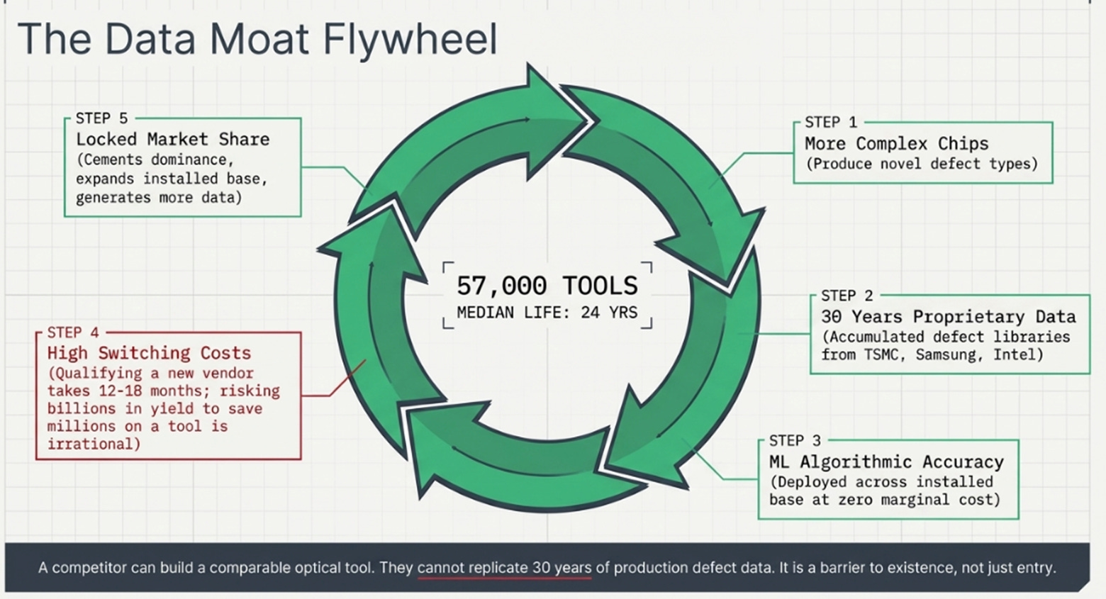
KLA has approximately 57,000 tools installed across every major fab on earth, with a median operating life of 24 years. These tools have accumulated three decades of proprietary defect libraries from TSMC, Samsung, Intel, SK Hynix, Micron, and dozens of smaller manufacturers. Each new generation of tools improves detection accuracy through machine learning algorithms trained on this data, and deploying those algorithms across the entire installed base carries zero marginal cost.
This creates something close to a compounding industrial learning system. More complex chips produce more novel defect types. More defect types generate more proprietary data. More data improves algorithmic accuracy. Better accuracy increases switching costs, qualifying a new inspection vendor takes 12 to 18 months and directly risks production yield, making no fab manager willing to gamble billions in yield loss to save a few million on tool capital expenditure. Higher switching costs cement market share. Larger market share expands the installed base. And a larger installed base generates more service revenue, more customer touchpoints, and more data, restarting the loop.
A competitor can theoretically build a comparable optical inspection tool. They cannot replicate 30 years of production defect data from every advanced fab on earth. This is not a barrier to entry. It is a barrier to existence.
The market sees a better semiconductor equipment company. The deeper reality is a better business model.
The Price of the Physics Tax
Everything described above is real. The structural dynamics are genuine. The compounding mechanism is durable. And nearly all of it is already in the stock price.
At 49 times trailing earnings and approximately 36 times forward earnings, KLA trades at 75% above its 10-year average price-to-earnings ratio. The stock has doubled in the past year. Every independent probability-weighted three-year price target I have encountered, from institutional research, from independent analysts, from my own scenario work, converges on a range of $1,470 to $1,693. The stock trades at $1,727.
The positioning data confirms the crowding. KLA is the number-one most overweight semiconductor stock among active fund managers, according to Bank of America’s February survey. “Long global semiconductors” is tied as the single most crowded trade on Wall Street, cited by 35% of survey respondents. Short interest has collapsed 27% from January to February, falling to just 2.2% of float. Bears have capitulated. There are no contrarians left to be proven wrong.
Insider activity is uniformly in one direction. CEO Rick Wallace sold approximately $22.9 million in shares over the past six months. CFO Bren Higgins sold approximately $4.8 million. EVP Brian Lorig sold approximately $7.4 million. No insider purchases have been detected. While insider selling at all-time highs is common and often programmatic, the complete absence of buying is notable for a management team that publicly presented a target of $84 in earnings per share by 2030 at their March investor day.
The January earnings report demonstrated exactly how this dynamic plays out in practice. KLA beat revenue estimates by 1.4%, beat earnings per share estimates, and guided the next quarter above consensus. The stock fell 15% over the following sessions. At these multiples, execution gets punished. Only acceleration gets rewarded.
The business case and the stock case have diverged. The business is getting structurally stronger. The stock has already capitalized that strength.
Three Scenarios
The range of outcomes over the next three years depends almost entirely on two variables: the trajectory of wafer fab equipment spending and the terminal multiple the market assigns to KLA’s earnings stream. The business fundamentals, share, intensity, services, are relatively stable across scenarios. What changes is the macro and the market’s willingness to pay.
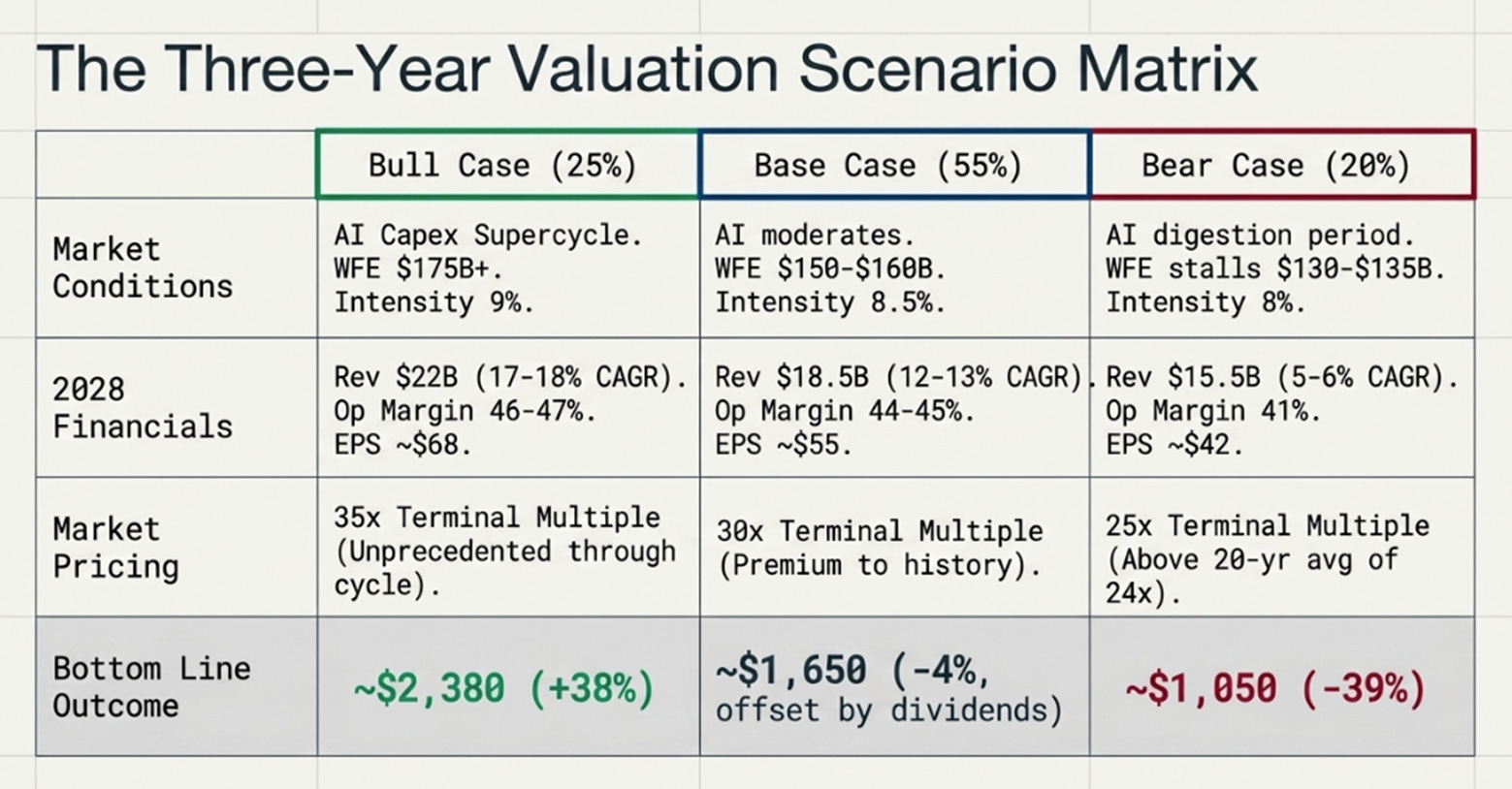
Bull Case (25% probability)
The AI capital expenditure supercycle sustains through 2028. Wafer fab equipment spending reaches $175 billion or more. Process control intensity accelerates toward 9% ahead of schedule as 2-nanometer yields prove more difficult than expected, forcing near-100% inline inspection at critical layers. Advanced packaging revenue exceeds $2 billion. Services track toward the $6 billion target.
Under these assumptions, KLA reaches approximately $22 billion in revenue by calendar year 2028, with operating margins expanding to 46 to 47% and non-GAAP earnings per share of roughly $68. If the market sustains a 35 times forward multiple, consistent with a monopoly whose cyclicality is demonstrably declining, the stock reaches approximately $2,380. That is a 38% return from current levels.
This requires management’s 2030 targets to be on track and the market to sustain a premium multiple through a full cycle. This combination has no precedent in semicap history.
Revenue CAGR: 17 to 18%. Operating margin: 46 to 47%. Terminal multiple: 35 times.
Base Case (55% probability)
AI spending continues but moderates. Wafer fab equipment grows at high-single-digit rates to $150 to $160 billion. Process control intensity reaches approximately 8.5% by 2028. China stabilizes at 20 to 25% of revenue. Advanced packaging reaches $1.5 to $1.8 billion. Services reach approximately $4.5 billion, tracking toward but not yet at the 2030 target.
Revenue reaches approximately $18.5 billion by 2028. Operating margins remain stable at 44 to 45%. Earnings per share reach approximately $55. At a 30 times forward multiple, a premium to history but below the current level, the stock trades at approximately $1,650. That is a 4% decline from today, roughly offset by cumulative dividends.
The business executes well. The stock goes approximately nowhere because the current multiple already embeds this outcome.
Revenue CAGR: 12 to 13%. Operating margin: 44 to 45%. Terminal multiple: 30 times.
Bear Case (20% probability)
The AI capital expenditure cycle experiences a digestion period in 2027 to 2028, consistent with Gartner’s repeated flagging of this risk window. Wafer fab equipment stagnates at $130 to $135 billion. Further export controls, potentially including the proposed MATCH Act’s retroactive prohibition on servicing existing tools in Chinese fabs, sever a portion of KLA’s highest-margin recurring revenue. Process control intensity stalls at approximately 8% as foundries delay advanced node migrations to conserve capital.
Revenue stagnates near $15.5 billion. Operating margins compress to 41% as fixed R&D costs deleverage. Earnings per share reach approximately $42. The multiple compresses to 25 times forward, still above the 20-year average of 24 times, reflecting the structural improvements in the business. The stock trades at approximately $1,050. That is a 39% decline.
Revenue CAGR: 5 to 6%. Operating margin: 41%. Terminal multiple: 25 times.
The Thesis Scoreboard
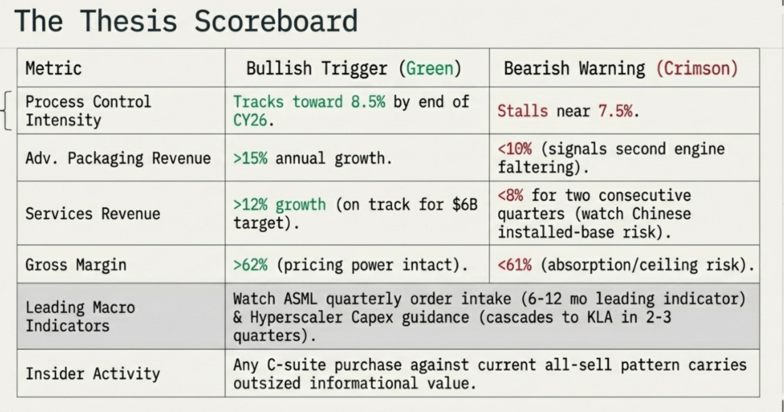
Seven metrics will determine which scenario is unfolding, listed in order of importance.
Process control intensity as a percentage of wafer fab equipment spending is the single most important number. If it approaches 8.5% by the end of calendar year 2026, the structural case strengthens materially. If it stalls near 7.5%, the thesis weakens.
Advanced packaging revenue trajectory must sustain growth above 15% annually. Any deceleration below 10% signals the second engine is faltering.
Services revenue growth rate must remain above 12% to track toward the $6 billion 2030 target. If growth drops below 8% for two consecutive quarters, particularly due to lost Chinese installed-base access, the compounding thesis weakens.
Gross margin trajectory above 62% signals pricing power is intact and tariff and component cost headwinds are being passed through. Below 61% signals absorption and margin ceiling risk.
ASML’s quarterly order intake is the most reliable leading indicator of wafer fab equipment direction six to twelve months forward.
Hyperscaler capital expenditure guidance from Microsoft, Google, Meta, and Amazon cascades to TSMC and then to KLA within two to three quarters. Any synchronized downward revision is an early warning.
Insider buying would be the most powerful signal against the current all-sell pattern. Any C-suite purchase, of any size, from a management team guiding to $84 earnings per share, would carry outsized informational value.
The Inspector’s Dilemma
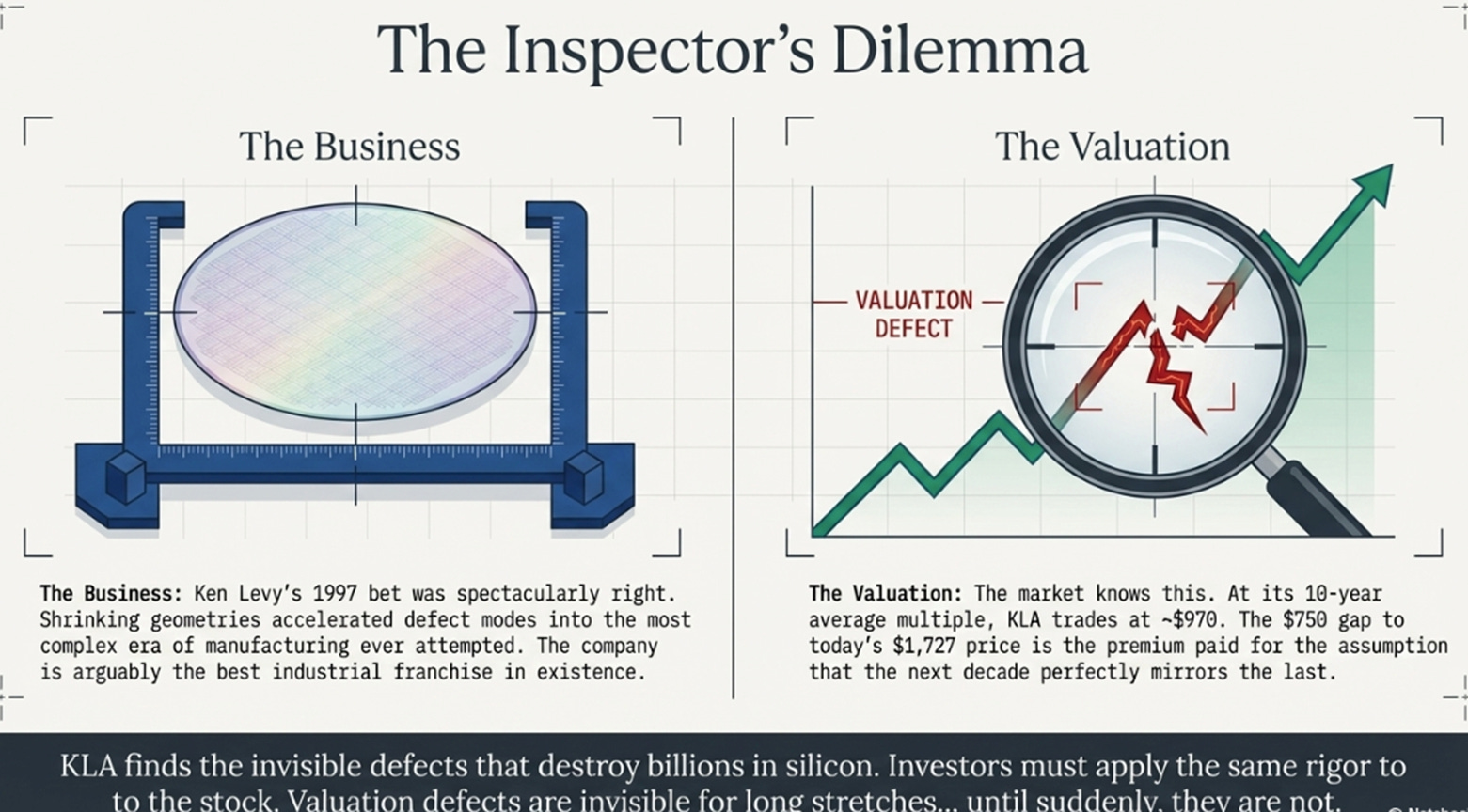
In 1997, Ken Levy bet that physics would make inspection indispensable. He was right, spectacularly, permanently, comprehensively right. KLA’s market position today is stronger than at any point in its history. Its addressable market is growing faster than the industry it serves. Its financial model produces margins and returns on capital that rival the best businesses in technology. And the same dynamic that made KLA essential 29 years ago, shrinking geometries creating more defect modes, is accelerating into the most complex era of semiconductor manufacturing ever attempted.
But here is the irony that Levy’s successors must contend with. The very qualities that make KLA an extraordinary business, dominant share, rising intensity, compounding services, a deepening data moat, have become so widely recognized that the stock market has priced them into a 49 times earnings multiple. At the 10-year average multiple, KLA would trade at roughly $970. The $750 gap between $970 and $1,727 is the premium the market pays for the expectation that the next decade will look like the last.
KLA’s inspectors find the defects that would otherwise destroy billions of dollars in silicon. Investors should apply the same rigor to the stock. The business is getting better as the industry gets harder. The company may be one of the rare industrial franchises whose economics improve with every increase in manufacturing complexity, a toll on avoidable failure that chipmakers will pay in perpetuity because the cost of not paying is worse.
The question is whether that truth is still an insight, or already common knowledge embedded in a very demanding stock price. In semiconductor manufacturing, defects that escape inspection always matter eventually. In equity markets, valuation defects have the same property. They are invisible for long stretches. And then, quite suddenly, they are not.
Disclaimer:
The content does not constitute any kind of investment or financial advice. Kindly reach out to your advisor for any investment-related advice. Please refer to the tab “Legal | Disclaimer” to read the complete disclaimer.