

Lam Research: The Atomic Toll Booth
Why a misunderstood bottleneck makes Lam structurally more valuable than the market believes

TL;DR
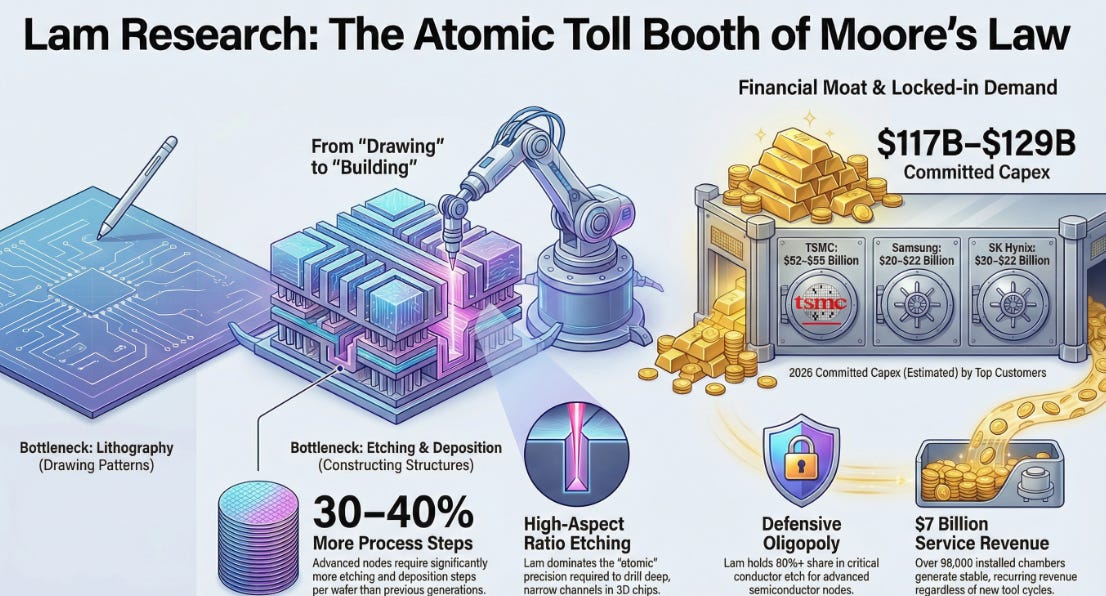
Advanced nodes now require 30–40% more process steps per wafer, centered on Lam’s strengths
Customer capex is already committed through 2027–28, locking in demand
Margins aren’t peaking, they’re normalizing higher as mix shifts to advanced nodes
The Promise That Wouldn’t Break
In 1965, Gordon Moore made a prediction that became a promise the industry made to itself: transistor density would double every 18 months, and compute cost would halve at the same pace. For sixty years, that promise held. Intel built tick-tock roadmaps around it. TSMC rose to dominance by delivering it. The entire digital age, smartphones, cloud computing, artificial intelligence, emerged because the semiconductor industry kept making things smaller.
Around 2020, that promise hit a wall. Not metaphorically, literally. TSMC engineers working on 3nm nodes encountered quantum tunneling effects where electrons simply jumped through barriers that were supposed to contain them. NAND architects faced aspect ratios in memory chips that defied conventional plasma chemistry. The math that had worked for six decades stopped working.
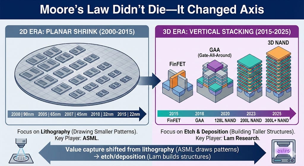
The industry didn’t break its promise. It changed the axis. If you can’t shrink in two dimensions, build in three. Planar transistors became FinFETs stacking silicon fins vertically, then Gate-All-Around structures layering nanosheets like a microscopic high-rise. NAND memory went from 64 layers to 300+. DRAM evolved into High Bandwidth Memory towers reaching 16 dies tall, connected by thousands of microscopic elevator shafts called through-silicon vias.
This transformation changed who collects the tolls. For decades, ASML commanded monopoly rents because lithography was the obvious constraint, you can’t build what you can’t draw. But drawing is just the blueprint. Someone still has to construct the structure: etch channels 50 times deeper than they are wide, deposit atomic layers inside trenches so narrow that conventional tools can’t reach them, drill through 50 micrometers of silicon while maintaining precision measured in nanometers.
That someone is Lam Research. And Wall Street still prices them like a cyclical tool vendor because it hasn’t realized the bottleneck, and thus the value capture, has permanently shifted from patterning to building.
The Fantasy Land Fallacy
In January 2026, TSMC’s CEO C.C. Wei told analysts something that should have been impossible: advanced computing revenue would grow at a 50% compound annual rate through 2029. Not 2026, when current fab projects complete. Not 2027, when the AI boom might moderate. Through 2029.
Run the physics. To support 50% annual revenue growth, that capacity needs to reach 350,000+ wafers monthly by 2029. You cannot conjure that supply from optimistic forecasts, it requires physical fabs, clean rooms, and thousands of process tools being installed right now.
The math compounds when you account for process intensity. A 2nm GAA wafer doesn’t just need the same tools as 3nm FinFET, it needs 15-20% more etch and deposition steps because the structures are more complex. HBM requires 3x the wafer input versus conventional DRAM for the same bit output, plus 4x the plasma etch intensity for those microscopic elevator shafts. A 300-layer NAND chip needs 50% more high-aspect-ratio etch time than a 200-layer chip because physics scales linearly when you’re drilling holes that deep.
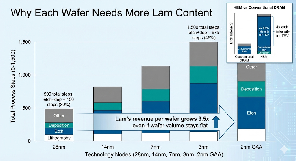
If compute demand grows 50% and each wafer requires 30-40% more process steps, equipment spending must grow 15-20% annually just to maintain the same output trajectory. Not cyclical recovery growth. Structural growth, sustained for years, or the compute scaling stops and the AI revolution stalls.
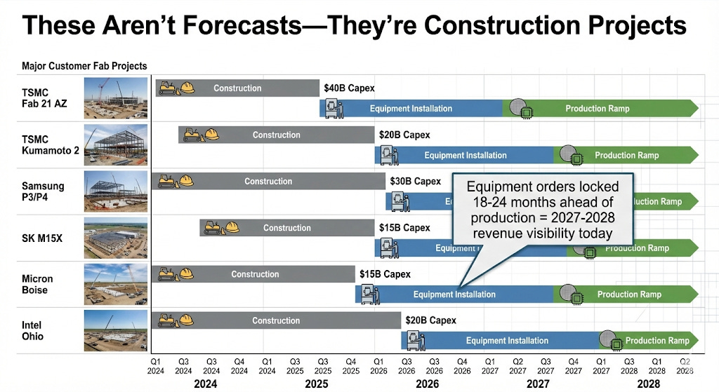
Wall Street models Lam’s revenue growing 8-10% annually, typical cyclical recovery rates based on 60 years of semiconductor equipment history. But TSMC just announced $52-56 billion in 2026 capital expenditures, up from $40 billion in 2025. That’s 30-40% growth. Samsung, SK Hynix, and Micron are guiding similar increases. These aren’t forecasts that might change if economic conditions deteriorate. The fabs are already under construction.
The Committed Capital Proof
In December 2024, TSMC broke ground on Fab 21 Phase 2 in Arizona, not a press release announcement, an actual groundbreaking with bulldozers and permits filed. Equipment installation begins Q3 2026 for 3nm production. The Kumamoto 2 fab in Japan has construction crews on-site today; equipment deliveries start Q1 2026. Samsung’s Pyeongtaek P3 and P4 memory fabs are ramping equipment installation through 2026-2027 for HBM production that customers have already contracted to buy. SK Hynix’s M15X fab in Cheongju completed construction in November 2025, with mass production scheduled for November 2026, eleven months from now. Micron’s Boise D1C facility and Idaho expansion are receiving EUV DRAM equipment deliveries as you read this.
Here’s the capital committed, not planned, committed, for 2026:
TSMC: $52-56 billion (confirmed January 2025 earnings call)
Samsung: $20-22 billion memory + foundry (announced October 2025 Capital Markets Day)
SK Hynix: $20-22 billion HBM-focused (Q3 2025 guidance, reiterated November)
Micron: $13-15 billion ramping 1γ/1δ DRAM (FY26 guidance)
Intel: $12-14 billion despite project delays (weighted toward equipment vs. construction)
Total: $117-129 billion from the top five customers alone, representing 20-30% growth year-over-year.
Semiconductor fabs take 18-24 months to fully equip after construction completes. Those 2026 spending commitments largely determine 2027-2028 equipment purchases. These aren’t demand forecasts that evaporate if consumer confidence weakens or enterprise IT budgets tighten. They’re purchase orders already placed or contractually committed under master supply agreements.
Lam’s September 2025 quarterly report showed $2.77 billion in backlog, up from $2.5 billion in June, that’s deferred revenue plus unfilled orders for work already contracted. At Lam’s current revenue run rate of approximately $21 billion annually, this represents 6-7 months of forward visibility. Combined with the customer capex commitments above, Lam’s revenue through mid-2027 is essentially locked.
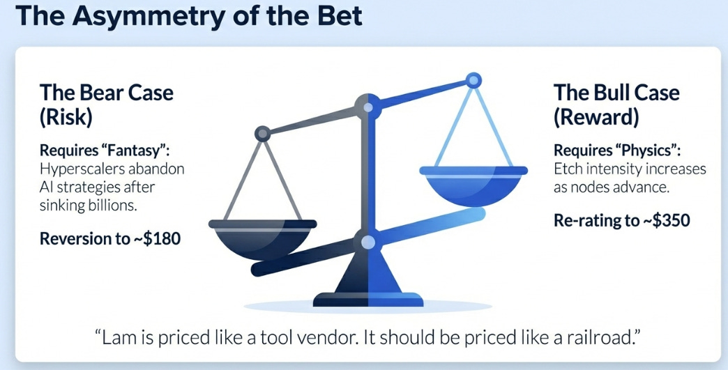
To believe the bear case, you’d need to believe that after spending $120+ billion in 2026 and installing equipment through 2027, these customers will suddenly abandon their AI strategies and slash spending in 2028. Why build the fabs if the demand isn’t real? Why sign hyperscaler offtake agreements for chip capacity years in advance if this is a bubble?
The committed capital makes the bear case require fantasy.
Why Competition Can’t Reach the Good Stuff
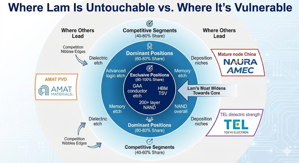
When you examine Lam’s competitive position, one pattern emerges: competitors can nibble at the edges, but they cannot touch what matters.
Tokyo Electron commands >50% market share in dielectric etch, the oxide and nitride insulating layers that support semiconductor structures. TEL’s Telius platform dominates through decades of process maturity and customer relationships. In this segment, Lam is the challenger. TEL also brings genuine innovation with its Nautilus cryogenic etch system for 3D NAND beyond 400 layers, claiming >2x throughput advantages. Samsung and SK Hynix are evaluating the tool.
But examine what TEL lacks: no credible conductor etch offering where Lam’s Akara and Kiyo platforms hold 80%+ share at advanced nodes. No TSV etch capability for HBM manufacturing where Lam’s Syndion is the exclusive supplier at both Samsung and SK Hynix. No services business integrated with process optimization the way Lam’s $7+ billion CSBG has become.
Customer procurement strategies reveal TEL’s actual role: the company serves as negotiating leverage for customers to extract better pricing from Lam, not as a preferred supplier customers choose for performance. Samsung leaks news of TEL cryo evaluations before Lam pricing negotiations. SK Hynix mentions “multi-vendor strategies” in investor presentations. Then they award 60-70% of volume to Lam anyway because when your $20 billion fab’s yield depends on a process step, you don’t optimize for tool cost, you optimize for outcomes.
Applied Materials occupies a different position: breadth without depth. AMAT commands ~40% of deposition equipment through leadership in PVD and CVD. The company monopolizes epitaxy for transistor source/drain regions. AMAT even has an etch business that crossed $1 billion quarterly revenue. But that $1 billion competes in niche applications, high-selectivity dielectric etch for specific memory types, specialized compound semiconductor processing, where Lam either doesn’t compete or chose not to invest.
TSMC’s 2nm process flow illustrates the dynamic: AMAT’s epitaxy for channel strain, AMAT’s PVD for metal barriers, AMAT’s high-κ dielectric deposition for gate stacks, and Lam’s etch for every conductor pattern that defines the transistor. The companies are complementary, not competitive. AMAT fills adjacent segments; Lam owns the critical path.
China’s semiconductor equipment industry has progressed faster than Western observers expected, but physics constrains what policy can accelerate. NAURA and AMEC now command 35-40% of equipment sales for mature nodes (≥28nm) in China, up from 2-5% five years ago. The government’s implicit 50% domestic equipment mandate accelerated adoption beyond what technical merit justified.
Yet advanced node manufacturing, where Lam generates highest margins and faces most inelastic demand, remains beyond Chinese capabilities. High aspect ratio etch for 3D NAND beyond 200 layers requires precise plasma chemistry control in trenches where sensors cannot reach. TSV etch for HBM requires drilling through 50+ micrometers of silicon while maintaining sidewall profiles that vary by less than 50 nanometers, deviations cause chip stacking failures that cascade through the entire die stack. GAA conductor etch must pattern features below 10 nanometers while preserving nanosheets only atoms thick.
These aren’t engineering challenges solvable through additional R&D funding. They require thousands of process iterations, deep partnerships with customers providing real production feedback, and integration of hardware, software, and process expertise accumulated over decades. Industry observers estimate Chinese vendors lag 5-7 years at advanced nodes, but this understates the challenge. By the time Chinese vendors master current capabilities, the frontier moves to backside power delivery, buried power rails, 3D DRAM, each introducing new physics that restart the learning cycle.
For Lam, China represents permanent loss of $3-4 billion in mature node revenue generating acceptable margins but no strategic differentiation. The advanced node revenue that drives competitive moats and pricing power remains secure through 2030 minimum.
The competitive reality: Lam retains 60-70% share through integration advantages and installed base effects, TEL captures 20-25% as credible alternative providing customer leverage, Chinese vendors displace mature node revenue that was never strategically critical. This is defensible oligopoly, not monopoly, but oligopoly is sufficient when you own the critical bottleneck.
The China Transition Nobody Understands
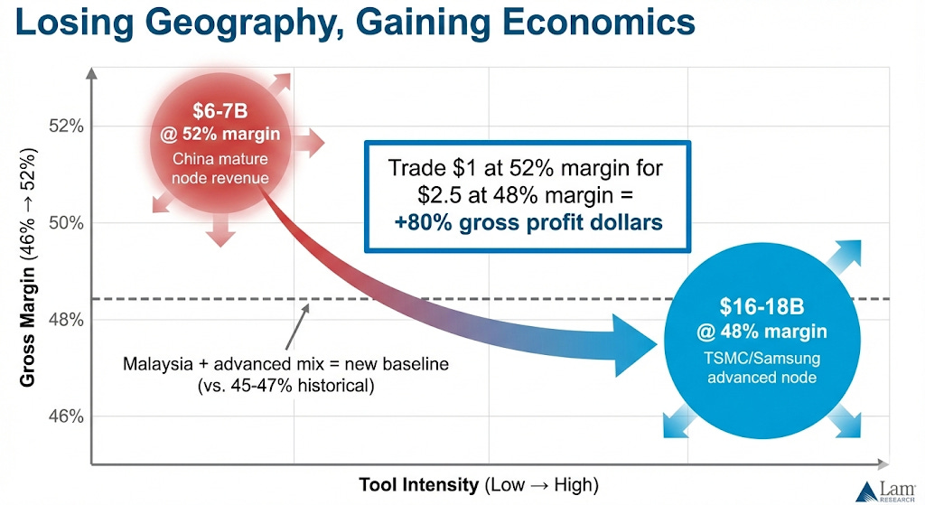
Wall Street’s primary anxiety is straightforward: China represented 43% of Lam’s revenue in June 2025, export controls force that below 30% by calendar 2026, a $2-3 billion revenue loss. How can the company grow with that headwind?
The answer lies in what’s being lost versus what’s being gained, and more importantly, what the margin compression actually reveals.
China revenue skewed toward mature nodes: 28nm to 90nm logic, commodity DRAM, earlier-generation NAND. Lower tool intensity applications where Lam’s Reliant etch systems and older deposition platforms compete. Gross margins were strong, approximately 52%, because Chinese customers had limited alternatives and paid full price.
The replacement revenue comes from TSMC’s 2nm ramp, Samsung’s HBM expansion, SK Hynix’s advanced DRAM nodes. These require latest-generation tools: Akara conductor etch for GAA transistors (launched February 2025), Syndion TSV etch for HBM (exclusive supplier position), Vector Strata ALD for 3D scaling, Cryo 3.0 etch enabling 200+ layer NAND. Gross margins on these tools run approximately 48%, lower than China due to customer concentration and volume pricing. But tool intensity is vastly higher. Where a mature node fab needs 15-20 Lam process tools, an advanced node fab needs 40-50.
The December 2025 guidance revealed the tension. Lam projected gross margins of 48.5% versus 50.6% in September, a 210 basis point step-down. CFO Doug Bettinger cited “customer concentration” as the primary driver. When he said that, he was using corporate code. Translation: TSMC and Samsung know Lam has no alternatives for certain critical steps, and they’re using that knowledge to negotiate aggressively. When you represent 60-70% of a supplier’s revenue, you have leverage regardless of their technical monopoly.
But the 48.5% floor isn’t arbitrary, it’s structural. Lam’s Malaysia manufacturing facility, fully ramped as of Q3 2025, contributes 100+ basis points of permanent improvement versus pre-2023 cost structure. Advanced node tool mix adds another 100-150 basis points compared to mature node blends. The China margin premium (52% vs 48%) masked these operational gains. As China normalizes, the Malaysia efficiency becomes visible for the first time.
Here’s what the market missed: margins aren’t compressing from peak to trough. They’re normalizing from artificially elevated (China premium concealing structural improvements) to sustainably higher (operational excellence on higher-value mix). The 48-49% range is still 300-400 basis points above Lam’s historical 45-47% range. That’s not cyclical margin peak, that’s permanent step-change.
And revenue guidance didn’t decline. For Q2 FY2026, Lam guided $5.2 billion, well above the Street’s $4.8 billion estimate. The December quarter guidance incorporated a $200 million impact from newly restricted customers, meaning underlying demand absorbed that hit and still grew.
Geography shifts. Margin quality adjusts. Volume overwhelms both.
The Coiled Spring
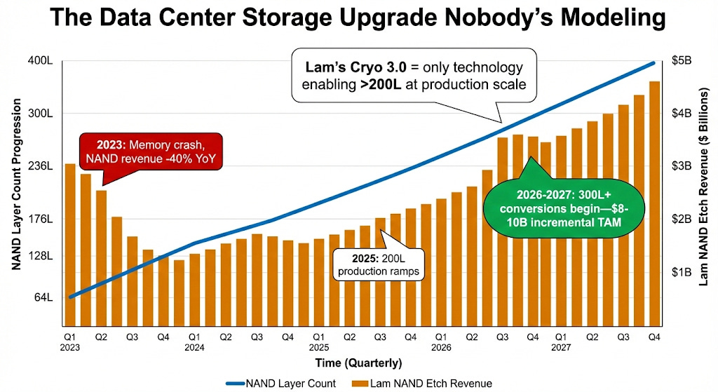
While Wall Street obsesses over logic and HBM, NAND sets up as the catalyst nobody’s modeling correctly for 2026-2027.
The data center storage upgrade cycle hasn’t started, it’s barely begun. Meta’s Llama training runs generate petabytes of checkpoint data requiring high-performance SSDs. Google’s Gemini workloads do the same. Enterprise storage is transitioning from 200-layer to 300-layer NAND not through firmware updates but through equipment upgrades, you cannot etch holes that deep with tools designed for shallower structures.
The total addressable market: approximately $40 billion over 3-4 years. Lam holds 65-70% market share in NAND etch, the critical bottleneck. The company’s Cryo 3.0 technology won the February 2025 SEMI Award by enabling 2.5x faster etch rates with 2x better profile precision for structures beyond 200 layers. This technology makes 300-layer NAND physically possible, aspect ratios reaching 50:1 require cryogenic temperatures to prevent sidewall damage during etching.
Management confirmed in September 2025 earnings that NAND would have “a good 2025 and a strong 2026.” Yet sell-side models show NAND as modest contributor, not major growth driver. Most analysts remain anchored to the 2023 memory crash when NAND revenue fell 40% year-over-year. They see the category through the lens of commodity cycles: oversupply, pricing collapse, capex cuts.
But this isn’t commodity NAND, it’s architectural upgrade NAND. Customers aren’t adding capacity speculatively; they’re converting existing fabs to new layer counts because old tools physically cannot build the structures next-generation products require. When Samsung moves from 236-layer to 321-layer NAND (announced for 2026 production), it’s not a choice, it’s the only way to maintain bit density roadmaps. When SK Hynix pushes beyond 300 layers, they need new etch chambers regardless of NAND pricing.
The setup is textbook: forgotten segment, structural catalyst, dominant market position, limited competition. When the NAND conversion cycle accelerates through 2026-2027, it layers on top of logic and DRAM growth already modeled. This isn’t replacing expected revenue, it’s adding to it.
Three Paths Forward
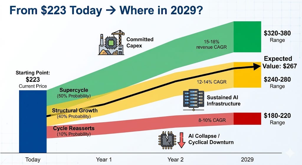
The Supercycle (50% probability): $320-380
Revenue grows 15-18% annually: FY26 $24-25B → FY29 $38-41B. TSMC maintains $54-58 billion annual capex through 2028. Memory makers sustain HBM investments as packaging bottlenecks resolve. NAND conversion cycle delivers $8-10 billion cumulative revenue over three years. Gross margins hold 50-51% as advanced node mix improves and customer concentration stabilizes.
FY29 EPS reaches $9.50-10.50. Multiple expands to 30-34x, not from hope, but from recognition that Lam operates a toll booth on Moore’s Law continuation with no viable alternatives. Stock trades $285-355.
This requires believing hyperscaler AI spending is competitive imperative, not discretionary investment. Microsoft, Google, Meta, Amazon are in prisoner’s dilemma: stop building, fall behind in AI capabilities. Keep building, collectively need the capacity. The $120+ billion committed for 2026 suggests they’ve made their choice.
Watch for:HBM4 substrate constraints resolving by mid-2026. DDR5 spot pricing holding above $55. Lam’s backlog growing sequentially.
Structural Growth (40% probability): $240-280
Revenue grows 12-14% annually: FY26 $23-24B → FY29 $33-36B. TSMC capex moderates to $52-54 billion range but stays elevated. Memory experiences soft patches but no crash. China restrictions remain at current levels without escalation. Gross margins settle at 48-49%.
FY29 EPS reaches $7.50-8.50. Multiple maintains 28-32x premium to historical averages, not from structural re-rating, but from sustained demonstration that this cycle has different characteristics than previous ones. Stock trades $210-270.
This is the “show me” scenario where market gradually accepts infrastructure narrative but demands proof each quarter. Conservative but rational.
Watch for: Customer capex steady around 2026 levels through 2027. Backlog flat to modest growth. Memory pricing soft ($48-52 DDR5) but stable. No new Entity List additions.
The Cycle Reasserts (10% probability): $180-220
Revenue grows 8-10% annually: FY26 $22-23B → FY29 $28-31B. TSMC cuts 2027 capex below $48 billion citing demand concerns. Memory pricing collapses (DDR5 under $45) as conventional DRAM oversupply emerges. Additional China restrictions remove another $1-2 billion. Gross margins compress toward 46-47% as customer concentration intensifies.
FY29 EPS reaches $6.00-7.00. Multiple contracts to 26-30x, slight premium to trough, acknowledging structural improvements but pricing for cyclical weakness. Stock trades $155-210.
This requires believing that after committing $120+ billion to fab construction in 2026 and installing equipment through 2027, hyperscalers materially reduce AI infrastructure spending in 2027-2028. Possible, but contradicted by offtake agreements already signed and competitive dynamics already established.
Would trigger on: TSMC using “normalizing” language in January 2026 guidance. Micron December 2025 earnings cutting FY26 capex below $13 billion. Lam’s April 2026 backlog declining more than 10% sequentially.
Current price $223 implies 20% upside to expected value over three years, approximately 6% annualized. Not cheap, not expensive. Fair value if you believe the base case. Compelling if you believe the supercycle. Dangerous if you believe the cycle reasserts.
The Signals That Matter
Don’t track fifty metrics. Track three that capture the essence:
TSMC 2027 capex guidance: Above $58 billion confirms supercycle. $52-56 billion sustains base case. Below $48 billion breaks thesis. This single number reveals whether hyperscalers believe in sustained AI infrastructure buildout or temporary spike.
Lam gross margin trajectory (quarterly): Sustained above 50% validates pricing power intact despite customer concentration. 48-49% confirms structural improvement with competitive pressure, acceptable. Below 47% signals customer concentration overwhelming economics, bearish.
Backlog sequential movement (quarterly): Growing confirms strong bookings pipeline and forward visibility. Flat acceptable with current high base. Declining 10%+ quarter-over-quarter is early warning signal that orders softening despite strong current revenue.
Completing Moore’s Promise
Gordon Moore’s 1965 prediction held for sixty years not because it was accurate forecasting, but because the industry committed to making it true. The promise became self-fulfilling: build roadmaps assuming compute cost halves every 18 months, invest accordingly, deliver the outcome. For six decades, that promise powered the digital revolution.
When physics blocked further shrinking around 2020, the casual observer might have declared Moore’s Law dead. The industry made a different choice: change the axis. Build in three dimensions. Stack transistors vertically. Etch channels fifty times deeper than they are wide. Deposit atomic layers in spaces where conventional tools cannot reach.
Lam Research operates the toll booth on this highway. Every advanced chip that ships, every NVIDIA H100 training AI models, every AMD MI300 powering cloud inference, every TSMC N2 processor enabling next-generation smartphones, carries the atomic tax that makes Moore’s Law continuation possible. The toll isn’t extractive; it reflects genuine value creation. But it is unavoidable.
TSMC has no alternative supplier for certain GAA etch steps. Samsung and SK Hynix have no other option for HBM through-silicon vias. The 96,000 chambers Lam has installed globally generate recurring service revenue for 10-15 years after initial sale, $7+ billion annually growing 12-16% even through downturns. Competitors can nibble at edges, but they cannot touch the core because the core requires decades of compound learning that cannot be replicated through additional investment alone.
Wall Street sees 45x earnings and thinks “late cycle peak.” That’s the category error. The market prices Lam like a tool vendor selling capital equipment in boom-bust cycles. But Lam isn’t selling tools, they’re selling the continued validity of Moore’s promise. And as long as AI requires exponential compute, someone has to collect the toll on that promise. The re-rating happens when the market recognizes this isn’t month 36 of a 48-month cycle but month 12 of a decade-long build.
At $223, Lam trades at a premium to its historical 22-24x average but below the 35-40x that ASML commands for lithography monopoly. The difference: ASML’s EUV has no competition. Lam faces Tokyo Electron in some segments, Applied Materials in others, Chinese vendors in mature nodes. Not monopoly, but infrastructure oligopoly where you own the critical bottleneck.
That’s sufficient. The railroad companies of the 1870s didn’t have monopolies, but they all compounded wealth for decades because the economy couldn’t function without rails. The cell tower operators of the 2000s competed with each other, but collectively captured value as mobile data exploded. Lam is the toll booth operator on Moore’s Law continuation. As long as AI demands exponential compute, the toll compounds.
The market will realize this when the committed capital becomes undeniable, when Q2 2026 earnings prove 48-49% margins are sustainable not cyclical, when 2027 plays out with TSMC maintaining $54+ billion capex rather than cutting. That’s when the multiple expands from 28-32x (cyclical premium) to 30-35x (infrastructure recognition).
If you’re buying Lam at $223, you’re not betting on hope. You’re betting on physics. The structures being built require Lam’s tools, the fabs under construction are real, the customer contracts are signed. The only question is whether Wall Street recognizes the bottleneck has moved before or after the revenue growth makes it obvious.
The asymmetry favors the buyer because the downside requires fantasy while the upside requires only that physics remains physics. Moore’s promise didn’t break. It evolved. And Lam Research collects the toll on that evolution.
Disclaimer:
The content does not constitute any kind of investment or financial advice. Kindly reach out to your advisor for any investment-related advice. Please refer to the tab “Legal | Disclaimer” to read the complete disclaimer.