

The Invisible Architect: How Cadence Quietly Became the Blueprint for the AI Era
From rubylith and X-acto knives to AI-designed silicon, Cadence Design Systems isn't just enabling chip innovation — it's redefining how compute gets built in a world where complexity is the constrain

Cadence is the foundational layer of modern compute, enabling the design of increasingly complex chips through its deeply integrated EDA, IP, and system analysis tools—effectively acting as the "blueprint architect" behind every AI, automotive, and custom silicon innovation.
Its strategic moat is built on irreplaceability, driven by high switching costs, co-development with chipmakers and foundries, and its dominance in analog design—making it one of the most defensible businesses in tech, regardless of semiconductor cycles.
Cadence is transitioning from vendor to infrastructure layer for the AI era, with AI-powered tools (like Cerebrus and JedAI), system-level expansion (SDA), and deepening relationships with hyperscalers and automakers unlocking new growth vectors beyond traditional chip design.

When Chips Were Built by Hand
Picture this: It's 1978, and inside a sterile room at Intel, an engineer named Dave hunches over a light table, squinting through a magnifying glass. In his hand, not a computer mouse or stylus, but an X-acto knife. Before him, sheets of red rubylith film—thin, translucent plastic that will become the pathways of tomorrow's microprocessors.
Layer by painstaking layer, he cuts and peels, creating the intricate patterns that will guide electrons through silicon. This wasn't a metaphor for precision work. This was literally how computer chips were designed: with hobby knives, tape, and the steady hands of engineers who understood that a single misplaced cut could doom months of work.
The red plastic sheets would be photographed, reduced, and etched onto silicon wafers. Each chip design was a physical artifact before it became a digital marvel. But Dave and his colleagues were racing against an inexorable force that would soon make their craft obsolete.
Every year, chips needed to pack more transistors into the same space. Every generation demanded more complexity, more precision, more speed. The human hand—no matter how steady, no matter how skilled—couldn't keep up with Moore's Law. Error rates exploded. Projects that should have taken months stretched into years. The semiconductor industry was approaching a wall that no amount of human skill could overcome.
The question wasn't whether this manual process would hit a limit—it was what would happen when it did. And whether the industry that had built the modern world could reinvent itself before that limit arrived
The Original Breakthrough: Cadence as a New Kind of Toolmaker

For decades, the answer seemed obvious to every major semiconductor company: build better internal tools. Intel, Motorola, Texas Instruments—each jealously guarded their proprietary design software like nuclear launch codes.
These tools were their competitive advantage, painstakingly developed by internal teams and never shared with competitors.
But by the early 1980s, a few visionaries began to see this vertical integration differently. What if the industry's obsession with proprietary design tools was actually holding everyone back?
The insight was radical: chip design had become too complex for any single company to master alone. The software needed to design a modern processor was becoming as sophisticated as the processor itself. Companies were spending fortunes building design tools instead of focusing on what made their chips unique.
This realization led to one of the most important mergers in tech history that nobody talks about. In 1988, SDA Systems and ECAD Inc. combined to form Cadence Design Systems. This wasn't just corporate consolidation—it represented a fundamental shift in how the semiconductor industry would operate.
Suddenly, the secret sauce was unbundled. Instead of every chip company building their own design tools, they could license world-class software from specialists whose only job was perfecting the design process. Engineers could focus on innovation instead of reinventing digital drafting tables.
Cadence wasn't making chips. It was making chipmaking possible for everyone. More importantly, it was creating the infrastructure that would allow Moore's Law to continue scaling from the inside—not just through manufacturing advances, but through design breakthroughs that made complexity manageable.
What Most People Still Get Wrong About Cadence
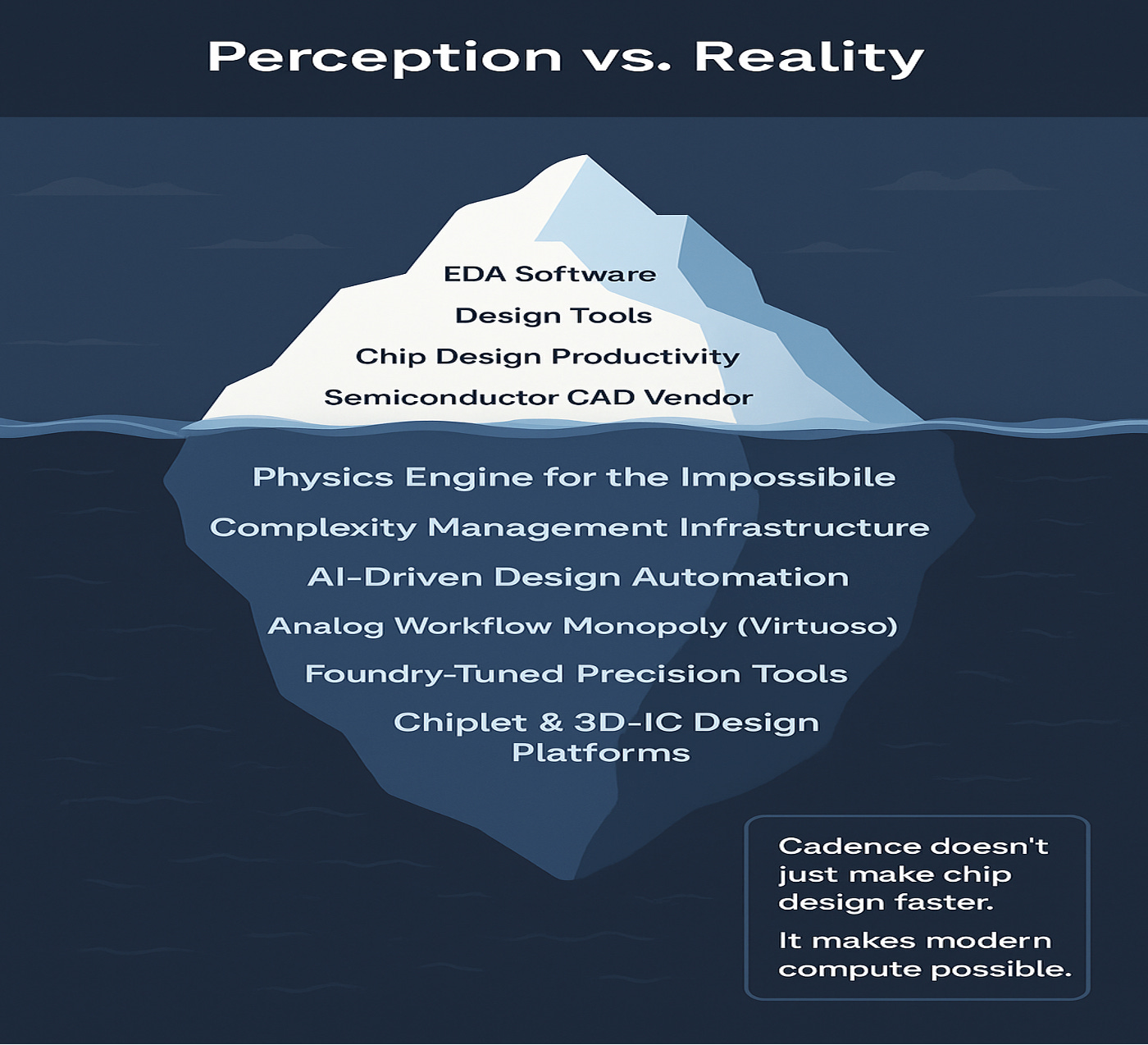
Walk into any investment meeting about Cadence, and you'll hear familiar refrains: "engineering software company," "semiconductor capital equipment," "tools for chip designers." These classifications miss something fundamental about what Cadence actually does and why it matters.
Most people see Cadence as benefiting from chip innovation. The reality is more profound: Cadence enables chip innovation. There's a crucial difference between riding industry trends and making those trends possible in the first place. Here's what the conventional view misses: the design phase is where everything that matters about a chip gets locked in. Performance, power consumption, security vulnerabilities, manufacturing yield—all of these are determined before a single transistor gets etched onto silicon. By the time a chip reaches a fabrication facility, 80% of its destiny has already been decided by the design tools that created it.
This isn't just software—it's the physics engine for the impossible. When NVIDIA designs a GPU with 76 billion transistors, engineers aren't drawing circuits on a screen. They're orchestrating a digital symphony where every note must be perfectly timed, every instrument precisely tuned, and every harmony mathematically verified before the first rehearsal.
The conventional analysis treats Cadence like a vendor selling productivity tools. But productivity tools help you do the same work faster. Cadence's tools help you do work that was previously impossible—designing chips so complex that no human team could ever verify their correctness without machine assistance.
That's not a software business. That's infrastructure for an entire technological civilization
The Quiet Transformation: From Workflow Vendor to AI Infrastructure Layer

While most observers focus on Cadence's traditional tools, something more fundamental has been happening in the background. The company isn't just adding AI features to existing software—it's building an entirely new intelligence layer that changes what chip design can accomplish.
Cerebrus and JedAI aren't upgrades. They're a different category of tool altogether. Traditional EDA software automates known processes—taking
human design intent and translating it into manufacturable layouts. AI-enhanced tools do something unprecedented: they explore design possibilities that no human engineer would ever consider.
Think about what this means in practice. A team designing a complex processor might spend months optimizing power consumption, trying dozens of layout configurations and timing adjustments. Cerebrus can evaluate millions of possibilities in the same timeframe, finding optimizations that human intuition would never discover.
One customer used Cerebrus to optimize a complex processor design in just 10 days—work that would have required several engineers several months to complete manually. But the AI didn't just save time; it found better solutions, identifying power and performance improvements that the original design team had missed entirely.
This creates a compounding effect that most analysis overlooks. Better chips require more sophisticated design tools. More sophisticated tools enable more complex chips. Cadence isn't just riding this cycle—it's accelerating it. Each breakthrough in AI-assisted design makes the next generation of processors possible, which in turn drives demand for even more powerful design tools.
The result is something approaching a technological feedback loop, with Cadence sitting at the center of an expanding spiral of capability and demand.
System Design: The Trojan Horse Expansion Strategy

Hidden within Cadence's financial reports is a business segment that most investors treat as a nice adjacency: System Design & Analysis (SDA). Growing at over 50% annually, SDA now represents 16% of total revenue, up from just 9% in 2020.
But calling SDA an adjacency misses its strategic significance. This isn't just another product line—it's a Trojan horse that transforms Cadence's entire relationship with its customers.
Traditional chip design ends when the digital blueprint is complete. SDA extends that relationship into the physical world. How does the chip behave when it heats up? What happens when electromagnetic interference disrupts signal timing? How does the processor interact with the circuit board, the cooling system, the power supply?
These aren't academic questions. A chip that works perfectly in simulation can
fail catastrophically when integrated into a real product. Tesla's autonomous driving computer doesn't just need to process neural networks efficiently—it needs to operate reliably at 85°C while vibrating down a highway, surrounded by electromagnetic interference from motors and sensors.
SDA tools model these real-world constraints before they become expensive failures. But here's the strategic insight: once a customer uses Cadence for system-level design, they're not just buying chip design tools anymore.
They're buying into a comprehensive platform that handles their entire electronic development process.
This dramatically expands wallet share without most customers realizing it's
happening. An automotive company might start with Cadence tools to design a
custom processor. But as they integrate that processor into vehicle systems,
they naturally expand into thermal modeling, electromagnetic simulation, and
power analysis. Each expansion deepens the integration and increases switching costs.
The market sees this as diversification. It's actually consolidation—of the customer's entire design workflow around a single platform provider.
The Strategic Moat No One Can Rip Out

Understanding Cadence's durability requires grasping a counterintuitive truth: the company's greatest asset isn't its technology—it's the workflow inertia it creates.
When a chip design team starts a project with Cadence's Genus synthesis tool, they're not just choosing software—they're choosing an entire design methodology. Genus naturally feeds into Innovus for physical layout, which seamlessly connects to Tempus for timing verification. This isn't just a toolchain; it's a design assembly line where removing any component would
stop the entire production line.
Switching tools mid-project is like performing heart surgery while the patient runs a marathon. Theoretically possible, practically insane. The cost isn't just the software licenses—it's the months of re-qualification, the risk of introducing new errors, and the productivity loss from engineers learning different methodologies.
But the lock-in goes deeper than workflow integration. Cadence has spent decades in symbiotic relationships with both chip designers and foundries, co-developing tools that are uniquely optimized for specific manufacturing processes. When TSMC develops a new 3-nanometer process, Cadence engineers work alongside TSMC's team to ensure perfect compatibility.
The result isn't generic software—it's a precision instrument calibrated for exact manufacturing conditions. Competitors can't simply replicate this because the optimization happens through years of collaboration, process refinement, and shared learning that can't be reverse-engineered or acquired.
Nowhere is this more apparent than in analog design, where Cadence's Virtuoso platform reigns virtually unchallenged. While digital circuits can often be reused across projects, analog circuits—which handle real-world signals like sound, power, and radio waves—must be custom-designed for each application and manufacturing process.
Virtuoso isn't just software; it's institutional memory crystallized into code. Design teams build entire libraries around it, develop custom methodologies, and train engineers in its specific approaches. Switching would mean abandoning years of accumulated expertise and starting over.
This creates an extraordinary business dynamic: Cadence's revenue is tied not to the volatile sales cycles of today's chips, but to the steady R&D budgets planning tomorrow's innovations.
The Strategic Context Has Shifted — and Cadence Is Sitting at the New Center
For its first two decades, Cadence primarily served the semiconductor industry's usual suspects: Intel, AMD, Qualcomm, and their peers. These were companies whose entire business model revolved around designing and selling chips.
Then something fundamental shifted. The biggest technology companies decided they couldn't wait for chip vendors to solve their problems—they would solve them internally.
Apple pioneered this transition with its A-series processors, custom silicon designed specifically for iPhones and iPads. The performance and efficiency gains were so dramatic that Apple eventually transitioned its entire Mac lineup to custom chips. Amazon followed with Graviton processors for AWS. Google
developed Tensor Processing Units for machine learning. Tesla created custom
chips for autonomous driving.
This wasn't just vertical integration—it was a recognition that in an AI-driven world, software and hardware must be co-designed to achieve breakthrough
performance. General-purpose processors, no matter how sophisticated,
couldn't match the efficiency of chips designed for specific workloads.
The implications for Cadence were profound. Suddenly, the customer base expanded from dozens of semiconductor firms to hundreds of system companies, each designing Application-Specific Integrated Circuits (ASICs)
tailored to their unique requirements.
But the expansion goes beyond technology companies. Defense contractors are designing custom chips for secure communications. Automotive companies are creating specialized processors for electric vehicles and autonomous systems. Even traditional industries like manufacturing and energy are discovering that custom silicon provides competitive advantages in efficiency and performance.
The geopolitical reshuffling of semiconductor supply chains makes this trend even more significant. As countries seek technological sovereignty, the ability to design custom chips becomes a matter of national security. Cadence's tools aren't just business infrastructure—they're the foundation for independent
technological capability.
Every nation that wants to participate in the AI revolution needs domestic chip design capability. And domestic chip design capability requires access to world-class design tools.

The Gap Between What It Is and What It's Seen As
Here's where the market's understanding diverges from reality. Most investors
still view Cadence as a slow-and-steady compounder—a defensive technology
stock that benefits from the semiconductor industry's long-term growth while
providing stability through economic cycles.
This classification made sense when Cadence was primarily selling traditional EDA tools to established chip companies. But it misses the second act that's currently unfolding: Cadence becoming central to how artificial intelligence
gets physically expressed in silicon.
Every breakthrough in AI—from large language models to autonomous vehicles to robotics—ultimately requires custom chips optimized for specific computational tasks. These aren't incremental improvements to existing processors; they're entirely new categories of silicon that push the boundaries of what's computationally possible.
Designing these chips requires tools that didn't exist five years ago. The traditional approach of human engineers manually optimizing layouts can't handle the complexity of modern AI accelerators. Machine learning models with billions of parameters require processors with architectural innovations that no previous generation of chips has attempted.
Cadence's AI-enhanced design tools aren't just helping customers build better versions of existing chips—they're enabling entirely new categories of silicon that would be impossible to design using traditional methods.
This structural shift isn't fully digested by the narrative or modeled in most financial projections. Analysts tend to extrapolate from historical growth rates and margin trends, missing the fundamental expansion in what Cadence makes possible for its customers.
The company is transitioning from selling productivity improvements to selling capability expansion. That's a different business model with different economics and different strategic value.

What to Watch
If this analysis is correct, certain metrics and developments should validate the
thesis over the coming quarters and years.
AI Tool Adoption and Usage Intensity: Track not just how many
customers license Cerebrus and JedAI, but how extensively they use
them. Real platform transformation shows up in usage metrics, not just
adoption rates. Look for customers expanding their AI tool usage across
multiple design projects and reporting productivity improvements that
justify premium pricing.System-Level Customer Growth: Monitor Cadence's expansion
beyond traditional semiconductor companies into automotive,
aerospace, and cloud infrastructure customers. These relationships start
with specific chip design projects but should evolve into comprehensive
platform partnerships that span multiple product categories.Foundry Partnership Depth: Watch for announcements of deeper
collaboration with TSMC, Samsung, and emerging foundries around AI-
optimized manufacturing processes. These partnerships create
competitive moats that extend beyond software into manufacturing
optimization.Cross-Selling and Platform Metrics: Pay attention to any disclosure
of customers using multiple Cadence product categories. Platform businesses succeed when they increase wallet share per customer, not
just customer count. Look for metrics showing the percentage of
customers using both traditional EDA tools and system-level design
capabilities.Geopolitical Navigation: Monitor how Cadence manages export
restrictions while expanding its role in regional design sovereignty
initiatives. The company's ability to serve domestic chip design
capabilities in multiple geographies without triggering additional
restrictions will be crucial for long-term growth.Competitive Response: Track whether Synopsys or other competitors
can match Cadence's integrated platform approach. Real competitive
advantages show up as sustained differentiation even when competitors
attempt to replicate successful strategies.
Most importantly, watch for evidence that Cadence's tools are enabling chip
designs that weren't previously possible, not just making existing designs
more efficient. That's the difference between incremental improvement and
fundamental capability expansion.
Conclusion: Cadence Is Not the Star, but It Is the Stage

In an industry obsessed with the latest breakthrough chip from NVIDIA or
Apple, Cadence represents something rarer and more valuable: the infrastructure that makes all breakthroughs possible.
The company never wanted to be the star of any story. While chip designers grab headlines and foundries get credit for manufacturing miracles, Cadence operates in the background, enabling both. This invisibility is intentional and incredibly valuable.
But invisibility doesn't mean insignificance. Every artificial intelligence breakthrough, every autonomous vehicle milestone, every quantum computing advance begins the same way: with engineers using Cadence tools to transform ideas into manufacturable reality.
The smartphone in your pocket contains chips designed with software that would have seemed like science fiction to the engineers cutting rubylith sheets in 1978. The data center processing this article relies on custom silicon optimized using AI algorithms that didn't exist a decade ago. The electric vehicle revolution depends on power management chips designed with thermal and electromagnetic modeling that enables new levels of efficiency and safety.
As the complexity of compute increases exponentially—from classical processors to AI accelerators to quantum circuits—the value of what Cadence builds increases along with it. The future of silicon will be defined before it's ever manufactured, in the digital realm where complexity becomes manageable and impossibility becomes routine.
And that's exactly where Cadence has been building its foundation for the past four decades: not as the star of the technological revolution, but as the indispensable stage where every breakthrough performance begins.
The tools may evolve from EDA to AI-assisted design to technologies we haven't yet imagined. The physics may shift from silicon to exotic materials and quantum effects. But the fundamental challenge remains unchanged:
making complexity tractable so that human ingenuity can continue pushing
the boundaries of what's possible.
In that ongoing project—the defining challenge of our technological civilization
—Cadence isn't just a participant. It's the architect of the blueprint itself.
Disclaimer:
The content does not constitute any kind of investment or financial advice. Kindly reach out to your advisor for any investment-related advice. Please refer to the tab “Legal | Disclaimer” to read the complete disclaimer.