

The Re-Bundling of Silicon
The next semiconductor battle is not inside the chip. It is around the package.

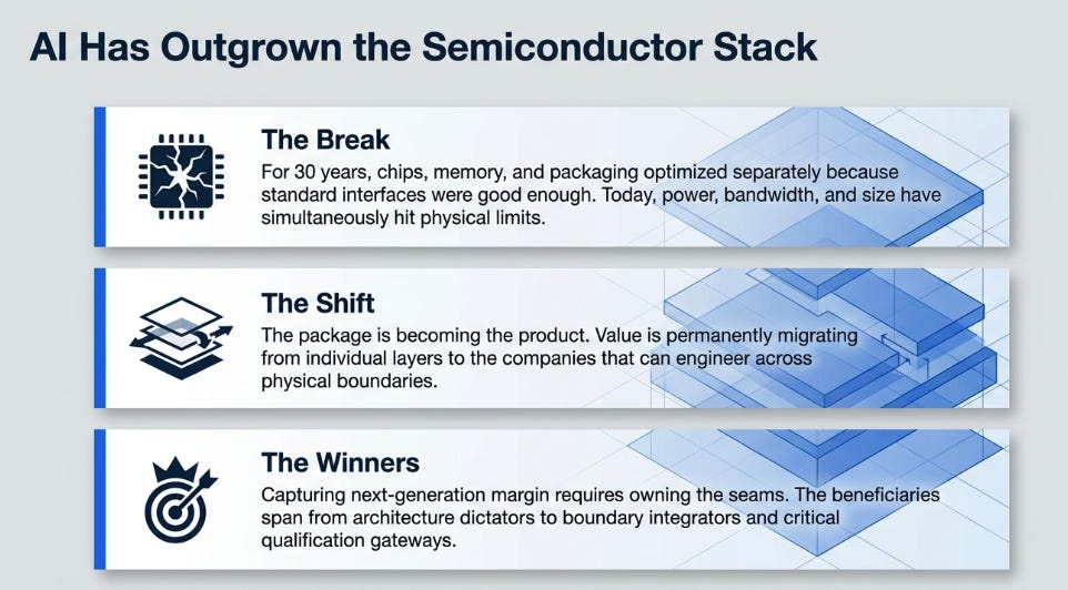
TL; DR:
AI has outgrown the old semiconductor model. For 30 years, chips, memory, packaging, and testing could be optimized separately because the interfaces between them were “good enough.” Power, bandwidth, and package size have now hit limits at the same time.
The package is becoming the product. Custom HBM, EMIB-T, microfluidic cooling, glass substrates, and advanced interconnects all point in the same direction: the value is shifting from individual layers to the companies that can integrate across boundaries.
The winners are not just Nvidia and TSMC. Nvidia defines the architecture, TSMC owns the deepest learning loop, but Marvell, Intel, SK Hynix, Samsung, Micron, and test/inspection players like Advantest and KLA may capture value where complexity becomes impossible to modularize.
The Dreamliner Problem
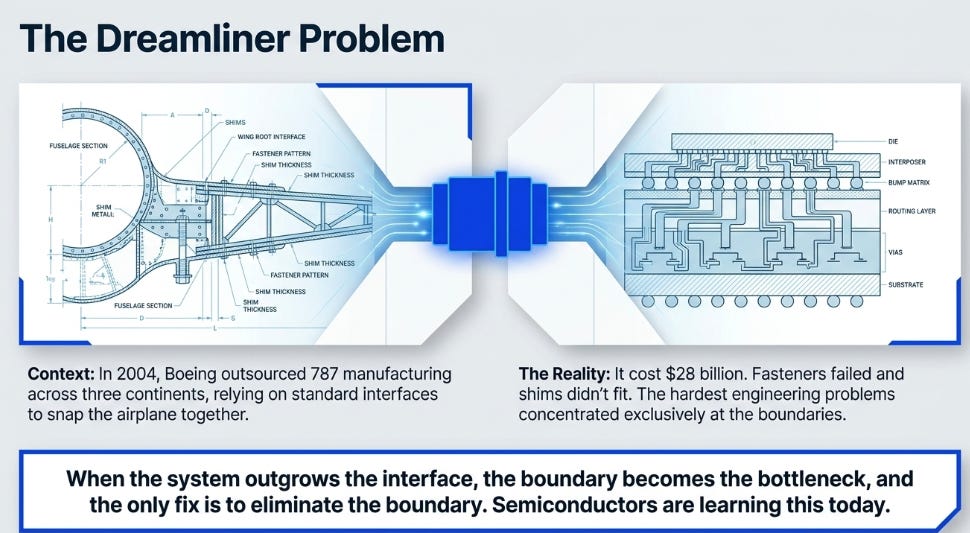
In 2004, Boeing made a decision that would cost it $28 billion and a decade of engineering credibility. The company decided to outsource the 787 Dreamliner’s manufacturing to a global network of suppliers. Each supplier would build a major structural section, fuselage barrels from Italy and Japan, wings from Mitsubishi, horizontal stabilizers from Alenia, and Boeing would snap them together at final assembly in Everett, Washington.
The logic was impeccable. Boeing’s core competence was systems integration, not fabricating carbon-fiber fuselage sections. Specialized suppliers could manufacture components more efficiently. Standardized interfaces at the joints between sections would ensure everything fit. Boeing had successfully disaggregated commercial aircraft production into modular, interchangeable layers connected by specifications.
The problem was that the specifications were inadequate for the system’s actual demands.
The joints between fuselage sections leaked. Shims that were supposed to fill gaps didn’t fit. Fasteners failed because the mating surfaces weren’t within tolerance. Wiring harnesses from one supplier didn’t align with connectors from another. Boeing engineers discovered that the hardest engineering problems were not inside any individual section, they were at the boundaries between sections. The interfaces that were supposed to be standardized turned out to be where system-level stress concentrated.
Boeing spent years and billions re-integrating. It acquired suppliers. It pulled manufacturing back in-house. It rebuilt the organizational knowledge that had been distributed across a dozen companies and three continents. The lesson was not that outsourcing was always wrong. The lesson was that unbundling works only when the interfaces between modules are adequate for the system’s demands. When the system outgrows the interface, the boundary becomes the bottleneck, and the only fix is to eliminate the boundary.
The semiconductor industry is now learning the same lesson.
The Great Unbundling
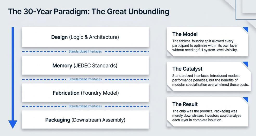
For thirty years, the semiconductor value chain has been one of the most successful examples of industrial unbundling in history.
The split happened in stages. TSMC, founded in 1987, separated chip design from chip manufacturing. The fabless-foundry model let companies like Nvidia and Qualcomm design processors without owning a fabrication plant. Outsourced semiconductor assembly and test companies, ASE, Amkor, SPIL, separated packaging from fabrication. JEDEC, the industry standards body, separated the memory interface from the processor design: any vendor’s HBM could plug into any compliant host.
Each act of unbundling created modular, interchangeable layers connected by standardized interfaces. The efficiency gains were enormous. Nvidia could iterate GPU architectures every two years without managing a fab. SK Hynix could manufacture HBM stacks without knowing what processor they would attach to. ASE could package chips without understanding their internal architecture. Every participant optimized within its own layer, and the standardized interfaces ensured the layers connected.
This worked for a specific reason that is easy to overlook: the interfaces were adequate.
A JEDEC HBM3 interface runs at 6.4 Gb/s per pin across a 1,024-bit bus. That is fast, but manageable with conventional interposer routing at standard line widths and spacing. Packages dissipated several hundred watts, within reach of standard cold plates and thermal interface materials. Silicon interposers fit within a single reticle, roughly 800 mm², on a standard 300mm circular wafer. The standardized boundaries between layers introduced modest performance penalties, but the benefits of modular specialization overwhelmed those costs.
The industry’s mental model followed the same structure. Investors asked which company had the best architecture, which foundry had the best node, which memory vendor had the most HBM capacity. The implicit assumption was that the layers could be analyzed separately. The chip was the product. Packaging was downstream.
That assumption is now wrong.
Three Walls at Once
ECTC, the Electronic Components and Technology Conference, is the packaging industry’s premier technical venue. The 2026 edition, held in Orlando in late May, featured major disclosures from Intel, TSMC, Samsung, Marvell, Lightmatter, Microsoft, and others. SemiAnalysis published a comprehensive roundup covering the most significant results. The individual technologies are interesting. Their shared direction is more important.
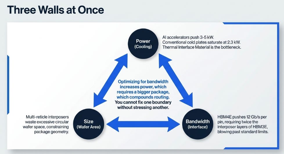
Three physical thresholds crossed simultaneously in 2025–2026, and the ECTC papers are the engineering receipts.
Power crossed cooling capacity. Samsung presented data showing HBM4E power consumption at 5.6 times HBM2 levels. Conventional lidded cold plate packages saturate at roughly 2.3 kW per package. Next-generation AI accelerators push toward 3–5 kW. Samsung’s own thermal analysis shows that 16-hi HBM stacks are near their thermal limits, and future 20-hi and 24-hi stacks are thermally unviable without fundamentally new cooling approaches. The thermal interface material between chip and heatsink, a layer the industry has relied on for decades, has become the bottleneck.
Bandwidth crossed interface capacity. HBM4E doubles pin count to 2,048 bits per stack and pushes per-pin data rates to 12 Gb/s and above. Samsung showed this requires twice the interposer layers compared to HBM3E and five times as many as HBM2. Meanwhile, Marvell demonstrated a custom HBM architecture achieving 64 Gb/s per pin using simultaneous bidirectional operation, five times the per-pin speed of standard HBM4E, while shortening the interposer channel from 6.5 mm to 1.5 mm. The gap between what the JEDEC standard specifies and what a co-optimized interface can deliver has become too large to ignore.
Size crossed wafer capacity. Next-generation accelerator packages need multi-reticle interposers, but circular silicon wafers constrain package geometry and waste edge area. Intel showed a 240 mm × 240 mm quarter-panel EMIB-T test vehicle equivalent to roughly 67 reticles. Resonac demonstrated panel-level processing on a 320 mm × 320 mm glass panel. ASE fabricated redistribution layers on a 600 mm × 600 mm panel.
Here is the critical point: these three thresholds interact. Optimizing the interposer for HBM4E bandwidth requires more routing layers, which increases power consumption, which exceeds thermal capacity. Adding more HBM stacks for memory capacity increases package size, which requires larger interposers, which compounds the routing and thermal problems. Improving cooling with microfluidic channels requires co-designing the cooling structure with the silicon die, which breaks the separation between chip design and thermal design. When every standardized interface hits its limit simultaneously, you cannot fix one boundary without stressing another.
The modular, unbundled model, where each layer optimized independently behind standard interfaces, cannot solve a problem that lives at the interaction between layers.
The question is no longer simply, who can design the fastest chip?
It is: who can make the fastest chip usable?
The Boundaries Dissolve
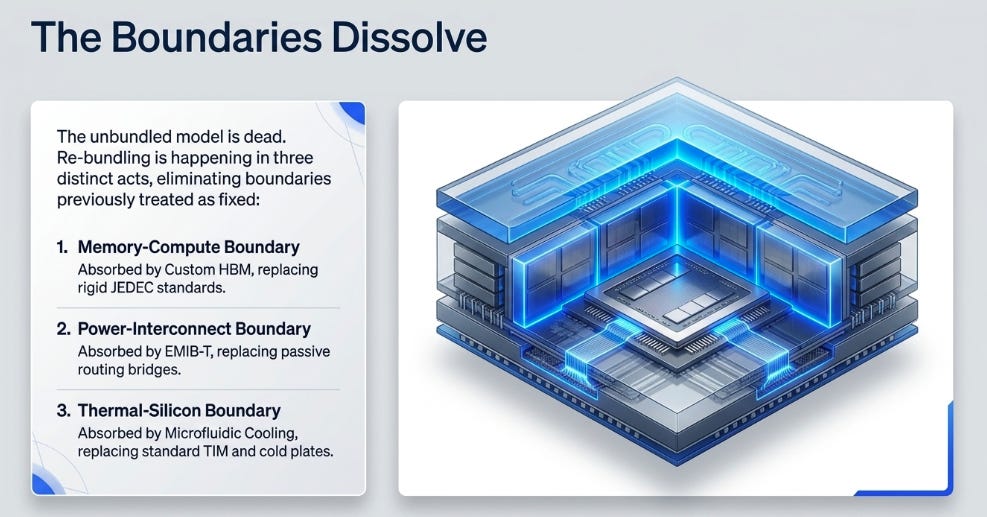
The re-bundling is happening in three acts, each eliminating a boundary that the unbundled model treated as fixed.
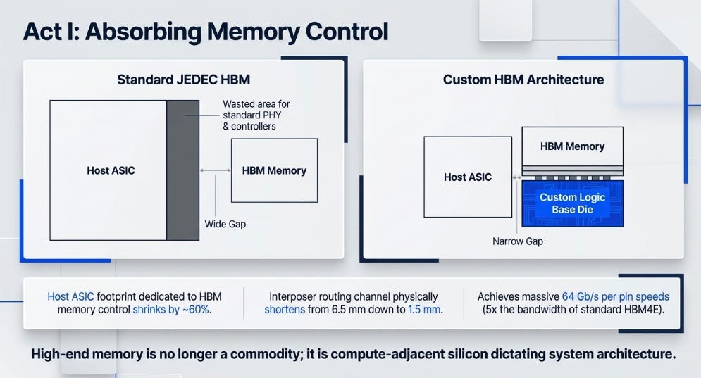
Custom HBM absorbs memory control into the HBM stack, breaking the JEDEC interface. For a decade, JEDEC defined how HBM connected to a host processor. Any vendor’s stack could pair with any compliant host. This interoperability was valuable, but it carried a structural cost: the host ASIC had to dedicate significant die area to HBM PHYs, controllers, and standardized pad placement. SemiAnalysis estimates that roughly 16% of Nvidia’s Rubin GPU die area goes to HBM-related logic.
Marvell’s custom HBM eliminates this boundary. The DRAM core dies stay the same. But the base die at the bottom of the stack becomes a custom logic chip, fabricated on an advanced process node, integrating the HBM controller, monitoring functions, custom logic, and expansion interfaces. The host ASIC no longer implements the standard PHY or routes a wide, fixed-pitch interface. Instead, base die and host communicate through an optimized die-to-die link co-designed for the specific accelerator.
The results are not incremental. Marvell claims the host ASIC footprint dedicated to HBM shrinks by roughly 60%. The interposer routing channel shortens from 6.5 mm to 1.5 mm. Bandwidth reaches 4.1 TB/s on an organic redistribution layer interposer rather than an expensive silicon one.
The deeper shift is architectural. The custom base die can act as a secondary memory controller and fan out to additional memory, LPDDR or even a second tier of HBM, without consuming the accelerator die’s scarce shoreline. Memory capacity scaling decouples from the compute die. Nvidia has confirmed that Feynman will use custom HBM. AMD’s future MI450 and MI500 will support LPDDR expansion. JEDEC will persist for mainstream applications, but for the highest-performance tier, the standard is becoming the legacy option.
That changes the memory value chain. If the base die carries the logic, HBM is no longer commodity memory priced by supply discipline. It is compute-adjacent silicon. Memory vendors face a structural choice: control the custom base die and capture system economics or supply interchangeable DRAM layers while someone else captures the interface margin.
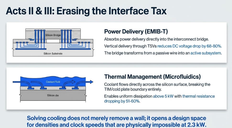
EMIB-T absorbs power delivery into the interconnect bridge, breaking the passive-bridge assumption. Intel’s EMIB has existed for years as a passive routing structure, a small silicon bridge embedded in the substrate connecting adjacent dies. EMIB-T adds through-silicon vias, transforming the bridge from a wire into a subsystem.
With TSVs, power can be delivered vertically through the bridge rather than laterally through the package around the bridge region. Intel claims this reduces DC voltage drop by 68–80%. The bridge now includes MIM capacitors at 500 nF/mm², improving power delivery network AC impedance by more than 82%. A 10-metal-layer stack carries both high-density signals and power simultaneously. Intel validated this at 36/35 µm bump pitch on packages with two reticles of silicon, with 4.5× reticle certification targeted by end of 2026 and 25 µm pitch test vehicles already running.
Intel’s roadmap extends this to higher-density MIM capacitors, active bridges, and embedded voltage regulators inside bridge dies, absorbing board-level and package-level functions into what was once the simplest element in the stack.
Microfluidic cooling absorbs thermal management into the silicon, breaking the TIM/cold plate boundary. TSMC formed silicon micropillars directly on the backside of SoC dies on a CoWoS-R test vehicle. Rather than transferring heat through thermal interface material to a lid to a cold plate, coolant flows directly across the silicon surface. Uniform power dissipation above 5 kW, continuing to scale with flow rate where conventional approaches plateau.
Microsoft went further by etching microchannels into an actual Nvidia GH200 GPU and running datacenter workloads for six months. GPU junction-to-inlet thermal resistance dropped 51–60%. Over roughly 4,370 observations, Microsoft recorded nine potential clogging events, declining over time, with no measurable silicon erosion.
Thermal interface material is literally an interface. AI turns that interface into a tax. Direct-to-silicon cooling is the removal of that tax.
But the deeper point is that solving cooling does not merely remove a wall, it opens a design space. A package that dissipates 5 kW enables accelerator architectures that are physically impossible at 2.3 kW: higher clock speeds, denser compute, more HBM stacks, tighter integration. The companies that solve cooling do not just cool better. They can build things that thermally constrained competitors cannot.
Scale Teaches Physics
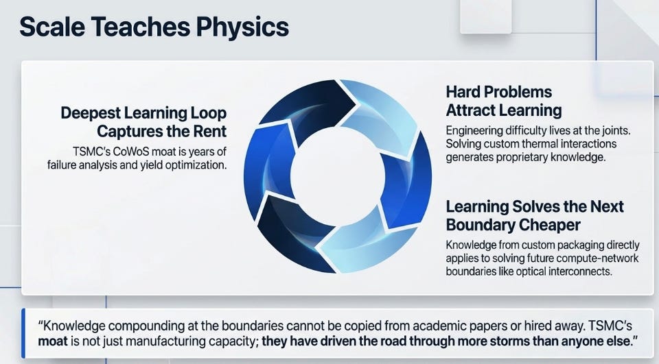
Boeing’s 787 lesson was that re-integration was not simply a manufacturing problem but a knowledge problem. The engineering difficulty lived at the joints, and the knowledge to solve those problems had been distributed across suppliers who each optimized within their own section. Re-integrating required rebuilding institutional knowledge that no single participant possessed.
The same dynamic applies to advanced packaging. Solving the memory-compute boundary (custom HBM) generates knowledge about signal integrity at short channel lengths, thermal interaction between logic base dies and DRAM stacks, and expansion interface protocols. That knowledge directly applies to solving the compute-network boundary (optical interconnects) because the same organic RDL interposer, thermal constraints, and die-to-die protocol challenges recur. Each boundary solved makes the next one cheaper. Each customer that ships on the integrated platform generates yield data and failure-mode analysis that benefit subsequent customers.
In software, the flywheel is data attracting users attracting more data. In AI hardware, the flywheel is problems attracting learning, learning attracting customers, and customers bringing harder problems. The company that has run the most advanced packages at the highest volume has accumulated knowledge that cannot be copied from published papers or hired away through talent acquisition. That knowledge compounds.
This is why TSMC remains formidable. Its learning loop around CoWoS is years deep. Every customer design teaches it something. Every manufacturing issue becomes process knowledge. Every generation strengthens the next. TSMC’s moat is not merely that it has the road. It is that it has driven the road through more storms than anyone else.
But learning loops can break. They break if interfaces re-standardize, if JEDEC catches up to custom HBM performance, the proprietary advantage dissipates. They break if customers internalize the learning, if Nvidia designs its own base die and builds its own packaging knowledge, Marvell’s platform value erodes. They break if a new architecture reduces package complexity, if a single-layer breakthrough in cooling or memory bandwidth removes the boundary cost without co-optimization. They break if geopolitics forces diversification despite inferior economics.
Until those conditions are met, the companies with the deepest learning loops capture the rent.
Who Owns the Seams
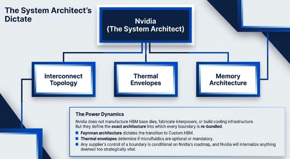
Before discussing the supply chain, the system architect deserves acknowledgment. Nvidia does not manufacture HBM base dies, fabricate interposers, or build cooling infrastructure. But Nvidia defines the architecture into which every boundary is re-bundled. It chose custom HBM for Feynman. Its thermal envelope determines whether microfluidic cooling is optional or necessary. Its interconnect topology dictates what bridges and interposers must support. Its roadmap cadence sets the timeline that every supplier designs against.
This is a different and arguably stronger form of power than controlling any individual boundary. Suppliers can capture rents at the seams, but Nvidia decides which seams exist and which are attacked first. Any supplier’s control of a given boundary is conditional on Nvidia’s architectural choices, and Nvidia has a track record of absorbing into its own silicon whatever it decides is too strategically important to outsource.
That said, re-bundling does create new positions of structural importance in the supply chain. Four companies illustrate the range.
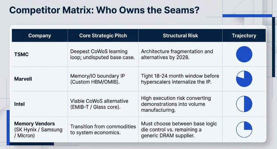
TSMC remains the base case. It owns the deepest packaging learning loop in the industry, years of CoWoS volume production, customer co-design, failure analysis, and yield optimization that no competitor can replicate from conference papers. Three ECTC trends structurally challenge CoWoS-S’s long-term position: custom HBM shortens interposer channels and enables organic RDL instead of silicon, panel-level organic interposers break the circular-wafer constraint, and embedded-bridge architectures reduce full-size interposer area. None of these displaces CoWoS for current products. But for the 2028–2029 generation, the packaging landscape fragments. TSMC presented three papers at ECTC. Intel presented twelve. That asymmetry is either strategic discipline or a misread of which competition matters next. Either way, TSMC remains the highest-quality compounder in this space because the learning loop is the hardest thing to replicate, and TSMC’s is the deepest.
Marvell is the most interesting company at the memory and I/O boundary. Custom HBM base die IP, OMIB optical interconnect bridge, Photonic Fabric chiplets, three points of control at the seams between major subsystems. But “interesting” is not “durable.” The central uncertainty is whether Marvell owns a reusable platform or provides bespoke integration work for customers powerful enough to eventually absorb the architecture. Nvidia will almost certainly design its own custom HBM base die for Feynman and beyond. Marvell’s window to establish custom HBM as a multi-customer platform, serving Google, Amazon, and other hyperscaler silicon programs alongside Nvidia, is roughly 18–24 months. If Marvell builds multi-customer breadth in that window, the platform becomes self-reinforcing: more customers amortize IP cost, generate learning, and make the next customer cheaper. If it remains a single-customer service, the most likely outcome is that the customer internalizes the capability and Marvell’s structural position weakens.
Intel has an opportunity most investors evaluate through the wrong lens. The conventional frame is Intel versus TSMC on leading-edge transistors, where Intel trails. The packaging frame is different. EMIB-T with integrated power delivery and MIM capacitors. A 510 mm × 515 mm, 24-layer glass-core panel with copper-filled through-glass vias, embedded EMIB bridges, and optical waveguides, an industry first, displayed at ECTC. Panel-level processing that breaks the circular wafer constraint. Ultra-low-temperature hybrid bonding at 175°C. Intel’s realistic pitch to hyperscalers is not “we are better than TSMC.” It is: “use us where dependence on CoWoS is too concentrated.” Hyperscalers do not want a single choke point. A second packaging platform with adequate capability but guaranteed capacity allocation may be worth more than waiting in TSMC’s queue. Google’s TPU v9 as an EMIB-T customer makes this concrete. But the warpage observed on Intel’s 240 mm × 240 mm test vehicle at the ECTC booth is not a small caveat, it goes directly to whether Intel can convert demonstration into volume manufacturing, which is exactly the transition Intel has failed repeatedly in recent years. EMIB-T is option value. It should be treated as such until volume yield proves otherwise.
SK Hynix, Samsung, and Micron face the structural choice that custom HBM forces on memory vendors. If they control the custom base die, its logic design, thermal behavior, expansion interfaces, and packaging integration, they move from component economics toward system economics. If they supply only DRAM layers while Marvell, Broadcom, or Nvidia controls the base die, they are pushed back toward commodity pricing. SK Hynix has the cleanest current HBM execution. Micron has significant earnings revision potential. Samsung’s memory-foundry-packaging combination becomes more strategically valuable as HBM base dies become more logic-rich, but only if Samsung can execute on integration, which its recent HBM track record does not yet prove.
What the Market Is Missing
The market’s first AI semiconductor framework was simple: Nvidia designs it, TSMC builds and packages it, SK Hynix supplies HBM. That framework was useful. It is now incomplete.
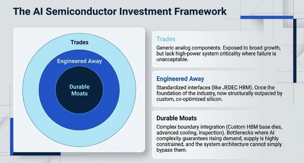
The better framework ranks bottlenecks by durability. A durable bottleneck has three properties: AI complexity increases the need for it every generation, supply cannot respond quickly, and the architecture cannot easily bypass it.
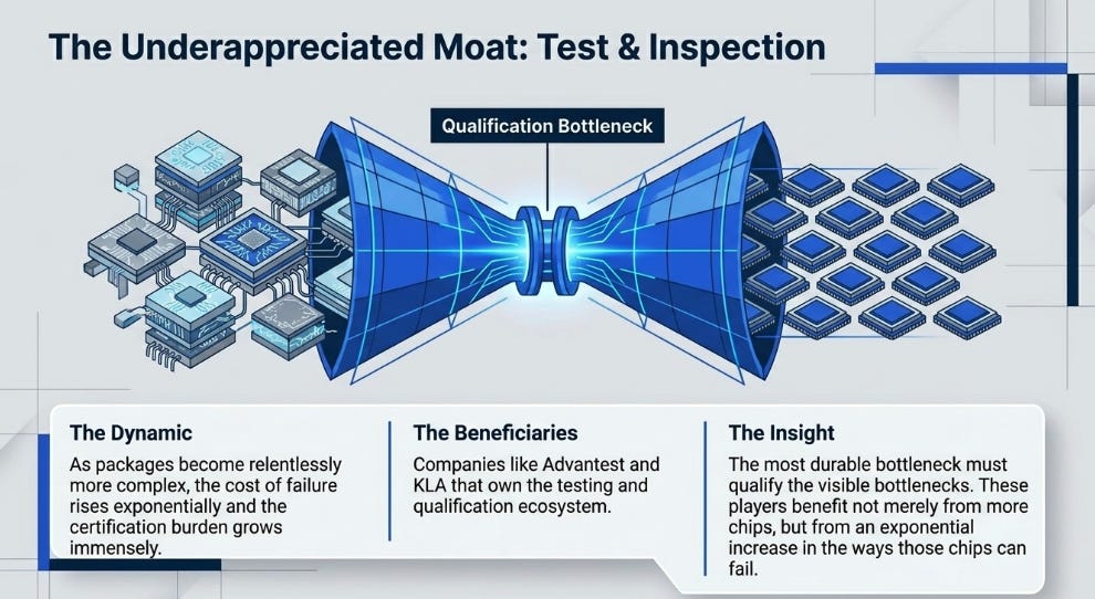
By that test, test, inspection, and qualification may be the most underappreciated layer. As packages become more complex, the cost of failure rises and the certification burden grows. Advantest, KLA, Teradyne, Onto, Camtek, and Disco benefit not merely from more chips but from more ways those chips can fail. The market likes visible bottlenecks. The more durable bottleneck may be the one that has to be qualified before the visible bottleneck can ship.
HBM and custom memory architecture remains the strongest near-term earnings-power layer. But it is no longer purely a cyclical memory call. Custom HBM makes memory vendors part of the architecture. The more logic, control, and expansion capability moves into the base die, the less HBM looks like commodity DRAM and the more it looks like differentiated silicon.
Power delivery and passives are real but require selectivity. Generic analog exposure is not AI-engine exposure. The distinction is whether a company sits in qualified, high-power system designs where failure is unacceptable, or merely sells components into a broadly growing market.
Optical interconnects and glass substrates are real technologies that should be option-sized until earnings timing is clearer. The more investable exposure runs through companies with revenue, manufacturing capability, and multiple paths to win rather than the purest concept stocks.
The portfolio mistake is buying every company adjacent to AI packaging. The edge is distinguishing between bottlenecks that become moats, bottlenecks that become trades, and bottlenecks that get engineered away.
The Call
The prediction is specific and can be proven wrong.
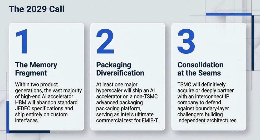
Within two product generations, by approximately 2029, the majority of high-end AI accelerator HBM will ship on custom, non-JEDEC interfaces. At least one major hyperscaler will be shipping an AI accelerator on a non-TSMC advanced packaging platform; if Intel cannot win that role, EMIB-T should be treated as technology without business proof. TSMC will respond to the fragmentation of packaging architectures by acquiring or deeply partnering with an interconnect IP company to match the boundary-layer integration that challengers are building independently.
The broader structural call: the semiconductor industry’s locus of value creation is migrating from transistor fabrication toward package-level integration. The companies that capture disproportionate value will be those that control the integration seams, the boundaries between memory and compute, between power delivery and interconnect, between thermal management and silicon, not the companies that excel at any single layer.
But control of the seams is not evenly distributed. Nvidia defines which seams exist and which are attacked first. TSMC owns the deepest learning loop for manufacturing across those seams. Marvell and Intel are the higher-upside challengers building alternative boundary architectures, each carrying meaningful execution risk. The memory vendors, SK Hynix, Samsung, Micron, face a structural fork between component economics and system economics, determined by whether they control the custom base die or merely supply the DRAM layers above it. And the test, inspection, and qualification companies sit where complexity becomes visible, growing more valuable with every new way a package can fail.
This can be wrong. JEDEC could remain dominant at the high end longer than expected. Custom HBM could prove too expensive or too fragmented. Microfluidic cooling could remain niche. Intel’s EMIB-T could fail to scale. The learning loops could break if customers internalize the knowledge or if a single-layer breakthrough eliminates the boundary cost.
But the direction is clear.
The semiconductor industry unbundled because the interfaces between layers were adequate for the system’s demands. AI broke that condition. The boundaries became the bottlenecks.
Boeing learned this at a cost of $28 billion and a decade.
The semiconductor industry is learning it now.
Disclaimer:
The content does not constitute any kind of investment or financial advice. Kindly reach out to your advisor for any investment-related advice. Please refer to the tab “Legal | Disclaimer” to read the complete disclaimer.